Table of contents
1. Introduction to SPI protocol
1. Introduction to SPI protocol
SPI (Serial Peripheral Interface) was developed by Motorola. It is not a standard protocol in the strict sense but almost all manufacturers comply with this protocol, so it can be said to be a "de facto" protocol. SPI is a synchronous four-wire full-duplex serial bus. The current speed can reach up to 50MHZ. It is also a master-slave structure. All transmissions are initiated through the host. However, unlike the I2C bus, the speed on the bus is There can only be one host controller. Each slave is selected through different chip select lines. The typical connection diagram is as shown in the figure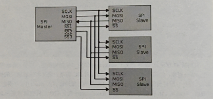
The Master is the master. There are 3 chip select signals SSI, SS2, and SS3, which are connected to 3 respectively. Slave, the chip select signal determines which slave is selected to communicate with it. The meanings of the 4 signal lines are as follows. SCLK (Serial Clock): Serial clock line, issued by the host.
MOSI (Master Output, Slave Input): Master output and slave input, that is, the line through which the master sends data and the slave receives data
MISO (Master Input, Slave Output): Master input and slave output, that is, the line through which the slave sends data and the host receives data
SS (Slave Select): Slave select line, sent by the host, active at low level.
Because the host can also receive data through MISO while sending data through MOSI, the SPI bus is full-duplex. All data is synchronized via the SCLK signal, so it is also a synchronous bus. A typical timing diagram of the SPI bus is shown in Figure. 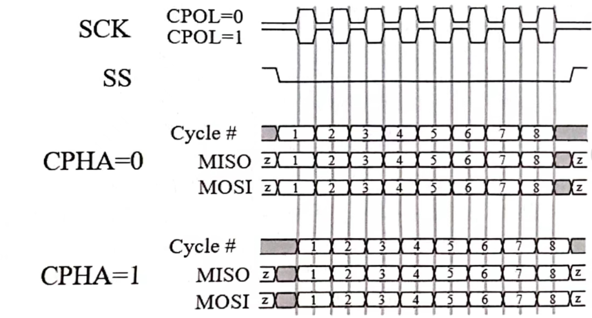
In the figure, CPOL represents the polarity of SCLK. A CPOL of 0 means that SCLK is usually low level, and a CPOL of 1 means that SCLK is usually high level. CPHA represents the SCLK phase when data is sampled. A CPHA of 0 means that the data is sampled on the leading edge of SCLK (which may be a rising edge or a falling edge) and the data is output on the trailing edge. A CPHA of 1 means that the data is output on the leading edge of SCLK and the trailing edge. Data collection. So there are the following four combinations.
CPOL=0, CPHA=0: SCLK is usually low level, the data of MISO is sampled on the rising edge of SCLK, and the data is output from MOSI on the falling edge of SCLK.
CPOL=0, CPHA=1: SCLK is usually low level, data is output from MOSI on the rising edge of SCLK, and MISO data is sampled on the falling edge of SCLK.
CPOL=1, CPHA=0: SCLK is usually high level. Data is output from MOSI on the rising edge of SCLK and MISO data is sampled on the falling edge of SCLK.
CPOL=1, CPHA=1: SCLK is usually high level, and MISO data is sampled on the rising edge of SCLK. Data is output from MOSI on the falling edge of SCLK.
If CPOL is used as the high bit of the mode and CPHA is used as the low bit of the mode, then the above four modes can be numbered as 0, 1, 2, and 3, among which mode 0 and mode 3 are commonly used modes.
2. Linux SPI driver
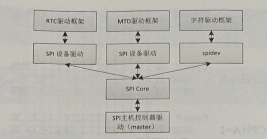
SPI driver and I2C driver are very similar. They both have host controller driver (called controller driver, and the host controller is called master in the driver), SPI Core and SPI device driver (called protocol driver), as shown in the figure below. The purpose of using this structure is also to separate the host and the device, so the SPI device driver does not need to care about the details of the host controller. Similarly, the host controller can also be implemented as a character device through spidev, so that the application program can directly control the SPI host controller to generate timing signals and achieve access to the SPI device. This application program is also called an application layer SPI device driver. . On top of the SPI device driver at the kernel layer are other driver frameworks used to implement specific device functions, such as RTC, MTD, etc.
SPI host controller drivers are generally implemented by SoC chip design manufacturers. We pay more attention to SPI device drivers. First, the representation method of SPI devices is explained. The corresponding structure types are defined as follows.
struct spi_device {
    struct device dev;
    struct spi_master *master;
    u32 max_speed_hz;
    u8 chip_select;
    u8 bits_per_word;
    u16 mode;
    int irq;
    void *controller_state;
    void *controller data;
    char modalias[SPI NAME SIZE];
    int cs_gpio;
};
The main members have the following meanings.
master: The connected SPI host controller.
max_speed_hz: The highest frequency at which the device operates.
chip_select: The chip select line used.
mode: The mode in which the device works.
cs_gpio: If the GPIO pin is used as the chip select signal, then cs_gpio is the GPIO pin number.
Like the I2C device driver, we usually do not construct the struct spi_device structure object directly, but describe the SPI device through the struct spi_board_info structure object, and use spi register_board_info to register the SPI device, such as in arch/arm/mach-s3c24xx/mach-jive.c There is the following code in it.
/* linux/arch/arm/mach-s3c2410/mach-jive.c
 *
 * Copyright 2007 Simtec Electronics
 *	Ben Dooks <[email protected]>
 *
 * http://armlinux.simtec.co.uk/
 *
 * This program is free software; you can redistribute it and/or modify
 * it under the terms of the GNU General Public License version 2 as
 * published by the Free Software Foundation.
*/

#include <linux/kernel.h>
#include <linux/types.h>
#include <linux/interrupt.h>
#include <linux/list.h>
#include <linux/timer.h>
#include <linux/init.h>
#include <linux/gpio.h>
#include <linux/syscore_ops.h>
#include <linux/serial_core.h>
#include <linux/platform_device.h>
#include <linux/i2c.h>

#include <video/ili9320.h>

#include <linux/spi/spi.h>
#include <linux/spi/spi_gpio.h>

#include <asm/mach/arch.h>
#include <asm/mach/map.h>
#include <asm/mach/irq.h>

#include <plat/regs-serial.h>
#include <linux/platform_data/mtd-nand-s3c2410.h>
#include <linux/platform_data/i2c-s3c2410.h>

#include <mach/regs-gpio.h>
#include <mach/regs-lcd.h>
#include <mach/fb.h>
#include <mach/gpio-samsung.h>

#include <asm/mach-types.h>

#include <linux/mtd/mtd.h>
#include <linux/mtd/nand.h>
#include <linux/mtd/nand_ecc.h>
#include <linux/mtd/partitions.h>

#include <plat/gpio-cfg.h>
#include <plat/clock.h>
#include <plat/devs.h>
#include <plat/cpu.h>
#include <plat/pm.h>
#include <linux/platform_data/usb-s3c2410_udc.h>
#include <plat/samsung-time.h>

#include "common.h"
#include "s3c2412-power.h"

static struct map_desc jive_iodesc[] __initdata = {
};

#define UCON S3C2410_UCON_DEFAULT
#define ULCON S3C2410_LCON_CS8 | S3C2410_LCON_PNONE
#define UFCON S3C2410_UFCON_RXTRIG8 | S3C2410_UFCON_FIFOMODE

static struct s3c2410_uartcfg jive_uartcfgs[] = {
	[0] = {
		.hwport	     = 0,
		.flags	     = 0,
		.ucon	     = UCON,
		.ulcon	     = ULCON,
		.ufcon	     = UFCON,
	},
	[1] = {
		.hwport	     = 1,
		.flags	     = 0,
		.ucon	     = UCON,
		.ulcon	     = ULCON,
		.ufcon	     = UFCON,
	},
	[2] = {
		.hwport	     = 2,
		.flags	     = 0,
		.ucon	     = UCON,
		.ulcon	     = ULCON,
		.ufcon	     = UFCON,
	}
};

/* Jive flash assignment
 *
 * 0x00000000-0x00028000 : uboot
 * 0x00028000-0x0002c000 : uboot env
 * 0x0002c000-0x00030000 : spare
 * 0x00030000-0x00200000 : zimage A
 * 0x00200000-0x01600000 : cramfs A
 * 0x01600000-0x017d0000 : zimage B
 * 0x017d0000-0x02bd0000 : cramfs B
 * 0x02bd0000-0x03fd0000 : yaffs
 */
static struct mtd_partition __initdata jive_imageA_nand_part[] = {

#ifdef CONFIG_MACH_JIVE_SHOW_BOOTLOADER
	/* Don't allow access to the bootloader from linux */
	{
		.name           = "uboot",
		.offset         = 0,
		.size           = (160 * SZ_1K),
		.mask_flags	= MTD_WRITEABLE, /* force read-only */
	},

	/* spare */
        {
                .name           = "spare",
                .offset         = (176 * SZ_1K),
                .size           = (16 * SZ_1K),
        },
#endif

	/* booted images */
        {
		.name		= "kernel (ro)",
		.offset		= (192 * SZ_1K),
		.size		= (SZ_2M) - (192 * SZ_1K),
		.mask_flags	= MTD_WRITEABLE, /* force read-only */
        }, {
                .name           = "root (ro)",
                .offset         = (SZ_2M),
                .size           = (20 * SZ_1M),
		.mask_flags	= MTD_WRITEABLE, /* force read-only */
        },

	/* yaffs */
	{
		.name		= "yaffs",
		.offset		= (44 * SZ_1M),
		.size		= (20 * SZ_1M),
	},

	/* bootloader environment */
	{
                .name		= "env",
		.offset		= (160 * SZ_1K),
		.size		= (16 * SZ_1K),
	},

	/* upgrade images */
        {
		.name		= "zimage",
		.offset		= (22 * SZ_1M),
		.size		= (2 * SZ_1M) - (192 * SZ_1K),
        }, {
		.name		= "cramfs",
		.offset		= (24 * SZ_1M) - (192*SZ_1K),
		.size		= (20 * SZ_1M),
        },
};

static struct mtd_partition __initdata jive_imageB_nand_part[] = {

#ifdef CONFIG_MACH_JIVE_SHOW_BOOTLOADER
	/* Don't allow access to the bootloader from linux */
	{
		.name           = "uboot",
		.offset         = 0,
		.size           = (160 * SZ_1K),
		.mask_flags	= MTD_WRITEABLE, /* force read-only */
	},

	/* spare */
        {
                .name           = "spare",
                .offset         = (176 * SZ_1K),
                .size           = (16 * SZ_1K),
        },
#endif

	/* booted images */
        {
		.name           = "kernel (ro)",
		.offset         = (22 * SZ_1M),
		.size           = (2 * SZ_1M) - (192 * SZ_1K),
		.mask_flags	= MTD_WRITEABLE, /* force read-only */
        },
	{
		.name		= "root (ro)",
		.offset		= (24 * SZ_1M) - (192 * SZ_1K),
                .size		= (20 * SZ_1M),
		.mask_flags	= MTD_WRITEABLE, /* force read-only */
	},

	/* yaffs */
	{
		.name		= "yaffs",
		.offset		= (44 * SZ_1M),
		.size		= (20 * SZ_1M),
        },

	/* bootloader environment */
	{
		.name		= "env",
		.offset		= (160 * SZ_1K),
		.size		= (16 * SZ_1K),
	},

	/* upgrade images */
	{
		.name		= "zimage",
		.offset		= (192 * SZ_1K),
		.size		= (2 * SZ_1M) - (192 * SZ_1K),
        }, {
		.name		= "cramfs",
		.offset		= (2 * SZ_1M),
		.size		= (20 * SZ_1M),
        },
};

static struct s3c2410_nand_set __initdata jive_nand_sets[] = {
	[0] = {
		.name           = "flash",
		.nr_chips       = 1,
		.nr_partitions  = ARRAY_SIZE(jive_imageA_nand_part),
		.partitions     = jive_imageA_nand_part,
	},
};

static struct s3c2410_platform_nand __initdata jive_nand_info = {
	/* set taken from osiris nand timings, possibly still conservative */
	.tacls		= 30,
	.twrph0		= 55,
	.twrph1		= 40,
	.sets		= jive_nand_sets,
	.nr_sets	= ARRAY_SIZE(jive_nand_sets),
};

static int __init jive_mtdset(char *options)
{
	struct s3c2410_nand_set *nand = &jive_nand_sets[0];
	unsigned long set;

	if (options == NULL || options[0] == '\0')
		return 0;

	if (strict_strtoul(options, 10, &set)) {
		printk(KERN_ERR "failed to parse mtdset=%s\n", options);
		return 0;
	}

	switch (set) {
	case 1:
		nand->nr_partitions = ARRAY_SIZE(jive_imageB_nand_part);
		nand->partitions = jive_imageB_nand_part;
	case 0:
		/* this is already setup in the nand info */
		break;
	default:
		printk(KERN_ERR "Unknown mtd set %ld specified,"
		       "using default.", set);
	}

	return 0;
}

/* parse the mtdset= option given to the kernel command line */
__setup("mtdset=", jive_mtdset);

/* LCD timing and setup */

#define LCD_XRES	 (240)
#define LCD_YRES	 (320)
#define LCD_LEFT_MARGIN  (12)
#define LCD_RIGHT_MARGIN (12)
#define LCD_LOWER_MARGIN (12)
#define LCD_UPPER_MARGIN (12)
#define LCD_VSYNC	 (2)
#define LCD_HSYNC	 (2)

#define LCD_REFRESH	 (60)

#define LCD_HTOT (LCD_HSYNC + LCD_LEFT_MARGIN + LCD_XRES + LCD_RIGHT_MARGIN)
#define LCD_VTOT (LCD_VSYNC + LCD_LOWER_MARGIN + LCD_YRES + LCD_UPPER_MARGIN)

static struct s3c2410fb_display jive_vgg2432a4_display[] = {
	[0] = {
		.width		= LCD_XRES,
		.height		= LCD_YRES,
		.xres		= LCD_XRES,
		.yres		= LCD_YRES,
		.left_margin	= LCD_LEFT_MARGIN,
		.right_margin	= LCD_RIGHT_MARGIN,
		.upper_margin	= LCD_UPPER_MARGIN,
		.lower_margin	= LCD_LOWER_MARGIN,
		.hsync_len	= LCD_HSYNC,
		.vsync_len	= LCD_VSYNC,

		.pixclock	= (1000000000000LL /
				   (LCD_REFRESH * LCD_HTOT * LCD_VTOT)),

		.bpp		= 16,
		.type		= (S3C2410_LCDCON1_TFT16BPP |
				   S3C2410_LCDCON1_TFT),

		.lcdcon5	= (S3C2410_LCDCON5_FRM565 |
				   S3C2410_LCDCON5_INVVLINE |
				   S3C2410_LCDCON5_INVVFRAME |
				   S3C2410_LCDCON5_INVVDEN |
				   S3C2410_LCDCON5_PWREN),
	},
};

/* todo - put into gpio header */

#define S3C2410_GPCCON_MASK(x)	(3 << ((x) * 2))
#define S3C2410_GPDCON_MASK(x)	(3 << ((x) * 2))

static struct s3c2410fb_mach_info jive_lcd_config = {
	.displays	 = jive_vgg2432a4_display,
	.num_displays	 = ARRAY_SIZE(jive_vgg2432a4_display),
	.default_display = 0,

	/* Enable VD[2..7], VD[10..15], VD[18..23] and VCLK, syncs, VDEN
	 * and disable the pull down resistors on pins we are using for LCD
	 * data. */

	.gpcup		= (0xf << 1) | (0x3f << 10),

	.gpccon		= (S3C2410_GPC1_VCLK   | S3C2410_GPC2_VLINE |
			   S3C2410_GPC3_VFRAME | S3C2410_GPC4_VM |
			   S3C2410_GPC10_VD2   | S3C2410_GPC11_VD3 |
			   S3C2410_GPC12_VD4   | S3C2410_GPC13_VD5 |
			   S3C2410_GPC14_VD6   | S3C2410_GPC15_VD7),

	.gpccon_mask	= (S3C2410_GPCCON_MASK(1)  | S3C2410_GPCCON_MASK(2)  |
			   S3C2410_GPCCON_MASK(3)  | S3C2410_GPCCON_MASK(4)  |
			   S3C2410_GPCCON_MASK(10) | S3C2410_GPCCON_MASK(11) |
			   S3C2410_GPCCON_MASK(12) | S3C2410_GPCCON_MASK(13) |
			   S3C2410_GPCCON_MASK(14) | S3C2410_GPCCON_MASK(15)),

	.gpdup		= (0x3f << 2) | (0x3f << 10),

	.gpdcon		= (S3C2410_GPD2_VD10  | S3C2410_GPD3_VD11 |
			   S3C2410_GPD4_VD12  | S3C2410_GPD5_VD13 |
			   S3C2410_GPD6_VD14  | S3C2410_GPD7_VD15 |
			   S3C2410_GPD10_VD18 | S3C2410_GPD11_VD19 |
			   S3C2410_GPD12_VD20 | S3C2410_GPD13_VD21 |
			   S3C2410_GPD14_VD22 | S3C2410_GPD15_VD23),

	.gpdcon_mask	= (S3C2410_GPDCON_MASK(2)  | S3C2410_GPDCON_MASK(3) |
			   S3C2410_GPDCON_MASK(4)  | S3C2410_GPDCON_MASK(5) |
			   S3C2410_GPDCON_MASK(6)  | S3C2410_GPDCON_MASK(7) |
			   S3C2410_GPDCON_MASK(10) | S3C2410_GPDCON_MASK(11)|
			   S3C2410_GPDCON_MASK(12) | S3C2410_GPDCON_MASK(13)|
			   S3C2410_GPDCON_MASK(14) | S3C2410_GPDCON_MASK(15)),
};

/* ILI9320 support. */

static void jive_lcm_reset(unsigned int set)
{
	printk(KERN_DEBUG "%s(%d)\n", __func__, set);

	gpio_set_value(S3C2410_GPG(13), set);
}

#undef LCD_UPPER_MARGIN
#define LCD_UPPER_MARGIN 2

static struct ili9320_platdata jive_lcm_config = {
	.hsize		= LCD_XRES,
	.vsize		= LCD_YRES,

	.reset		= jive_lcm_reset,
	.suspend	= ILI9320_SUSPEND_DEEP,

	.entry_mode	= ILI9320_ENTRYMODE_ID(3) | ILI9320_ENTRYMODE_BGR,
	.display2	= (ILI9320_DISPLAY2_FP(LCD_UPPER_MARGIN) |
			   ILI9320_DISPLAY2_BP(LCD_LOWER_MARGIN)),
	.display3	= 0x0,
	.display4	= 0x0,
	.rgb_if1	= (ILI9320_RGBIF1_RIM_RGB18 |
			   ILI9320_RGBIF1_RM | ILI9320_RGBIF1_CLK_RGBIF),
	.rgb_if2	= ILI9320_RGBIF2_DPL,
	.interface2	= 0x0,
	.interface3	= 0x3,
	.interface4	= (ILI9320_INTERFACE4_RTNE(16) |
			   ILI9320_INTERFACE4_DIVE(1)),
	.interface5	= 0x0,
	.interface6	= 0x0,
};

/* LCD SPI support */

static struct spi_gpio_platform_data jive_lcd_spi = {
	.sck		= S3C2410_GPG(8),
	.mosi		= S3C2410_GPB(8),
	.miso		= SPI_GPIO_NO_MISO,
};

static struct platform_device jive_device_lcdspi = {
	.name		= "spi-gpio",
	.id		= 1,
	.dev.platform_data = &jive_lcd_spi,
};


/* WM8750 audio code SPI definition */

static struct spi_gpio_platform_data jive_wm8750_spi = {
	.sck		= S3C2410_GPB(4),
	.mosi		= S3C2410_GPB(9),
	.miso		= SPI_GPIO_NO_MISO,
};

static struct platform_device jive_device_wm8750 = {
	.name		= "spi-gpio",
	.id		= 2,
	.dev.platform_data = &jive_wm8750_spi,
};

/* JIVE SPI devices. */

static struct spi_board_info __initdata jive_spi_devs[] = {
	[0] = {
		.modalias	= "VGG2432A4",
		.bus_num	= 1,
		.chip_select	= 0,
		.mode		= SPI_MODE_3,	/* CPOL=1, CPHA=1 */
		.max_speed_hz	= 100000,
		.platform_data	= &jive_lcm_config,
		.controller_data = (void *)S3C2410_GPB(7),
	}, {
		.modalias	= "WM8750",
		.bus_num	= 2,
		.chip_select	= 0,
		.mode		= SPI_MODE_0,	/* CPOL=0, CPHA=0 */
		.max_speed_hz	= 100000,
		.controller_data = (void *)S3C2410_GPH(10),
	},
};

/* I2C bus and device configuration. */

static struct s3c2410_platform_i2c jive_i2c_cfg __initdata = {
	.frequency	= 80 * 1000,
	.flags		= S3C_IICFLG_FILTER,
	.sda_delay	= 2,
};

static struct i2c_board_info jive_i2c_devs[] __initdata = {
	[0] = {
		I2C_BOARD_INFO("lis302dl", 0x1c),
		.irq	= IRQ_EINT14,
	},
};

/* The platform devices being used. */

static struct platform_device *jive_devices[] __initdata = {
	&s3c_device_ohci,
	&s3c_device_rtc,
	&s3c_device_wdt,
	&s3c_device_i2c0,
	&s3c_device_lcd,
	&jive_device_lcdspi,
	&jive_device_wm8750,
	&s3c_device_nand,
	&s3c_device_usbgadget,
	&s3c2412_device_dma,
};

static struct s3c2410_udc_mach_info jive_udc_cfg __initdata = {
	.vbus_pin	= S3C2410_GPG(1),		/* detect is on GPG1 */
};

/* Jive power management device */

#ifdef CONFIG_PM
static int jive_pm_suspend(void)
{
	/* Write the magic value u-boot uses to check for resume into
	 * the INFORM0 register, and ensure INFORM1 is set to the
	 * correct address to resume from. */

	__raw_writel(0x2BED, S3C2412_INFORM0);
	__raw_writel(virt_to_phys(s3c_cpu_resume), S3C2412_INFORM1);

	return 0;
}

static void jive_pm_resume(void)
{
	__raw_writel(0x0, S3C2412_INFORM0);
}

#else
#define jive_pm_suspend NULL
#define jive_pm_resume NULL
#endif

static struct syscore_ops jive_pm_syscore_ops = {
	.suspend	= jive_pm_suspend,
	.resume		= jive_pm_resume,
};

static void __init jive_map_io(void)
{
	s3c24xx_init_io(jive_iodesc, ARRAY_SIZE(jive_iodesc));
	s3c24xx_init_clocks(12000000);
	s3c24xx_init_uarts(jive_uartcfgs, ARRAY_SIZE(jive_uartcfgs));
	samsung_set_timer_source(SAMSUNG_PWM3, SAMSUNG_PWM4);
}

static void jive_power_off(void)
{
	printk(KERN_INFO "powering system down...\n");

	gpio_request_one(S3C2410_GPC(5), GPIOF_OUT_INIT_HIGH, NULL);
	gpio_free(S3C2410_GPC(5));
}

static void __init jive_machine_init(void)
{
	/* register system core operations for managing low level suspend */

	register_syscore_ops(&jive_pm_syscore_ops);

	/* write our sleep configurations for the IO. Pull down all unused
	 * IO, ensure that we have turned off all peripherals we do not
	 * need, and configure the ones we do need. */

	/* Port B sleep */

	__raw_writel(S3C2412_SLPCON_IN(0)   |
		     S3C2412_SLPCON_PULL(1) |
		     S3C2412_SLPCON_HIGH(2) |
		     S3C2412_SLPCON_PULL(3) |
		     S3C2412_SLPCON_PULL(4) |
		     S3C2412_SLPCON_PULL(5) |
		     S3C2412_SLPCON_PULL(6) |
		     S3C2412_SLPCON_HIGH(7) |
		     S3C2412_SLPCON_PULL(8) |
		     S3C2412_SLPCON_PULL(9) |
		     S3C2412_SLPCON_PULL(10), S3C2412_GPBSLPCON);

	/* Port C sleep */

	__raw_writel(S3C2412_SLPCON_PULL(0) |
		     S3C2412_SLPCON_PULL(1) |
		     S3C2412_SLPCON_PULL(2) |
		     S3C2412_SLPCON_PULL(3) |
		     S3C2412_SLPCON_PULL(4) |
		     S3C2412_SLPCON_PULL(5) |
		     S3C2412_SLPCON_LOW(6)  |
		     S3C2412_SLPCON_PULL(6) |
		     S3C2412_SLPCON_PULL(7) |
		     S3C2412_SLPCON_PULL(8) |
		     S3C2412_SLPCON_PULL(9) |
		     S3C2412_SLPCON_PULL(10) |
		     S3C2412_SLPCON_PULL(11) |
		     S3C2412_SLPCON_PULL(12) |
		     S3C2412_SLPCON_PULL(13) |
		     S3C2412_SLPCON_PULL(14) |
		     S3C2412_SLPCON_PULL(15), S3C2412_GPCSLPCON);

	/* Port D sleep */

	__raw_writel(S3C2412_SLPCON_ALL_PULL, S3C2412_GPDSLPCON);

	/* Port F sleep */

	__raw_writel(S3C2412_SLPCON_LOW(0)  |
		     S3C2412_SLPCON_LOW(1)  |
		     S3C2412_SLPCON_LOW(2)  |
		     S3C2412_SLPCON_EINT(3) |
		     S3C2412_SLPCON_EINT(4) |
		     S3C2412_SLPCON_EINT(5) |
		     S3C2412_SLPCON_EINT(6) |
		     S3C2412_SLPCON_EINT(7), S3C2412_GPFSLPCON);

	/* Port G sleep */

	__raw_writel(S3C2412_SLPCON_IN(0)    |
		     S3C2412_SLPCON_IN(1)    |
		     S3C2412_SLPCON_IN(2)    |
		     S3C2412_SLPCON_IN(3)    |
		     S3C2412_SLPCON_IN(4)    |
		     S3C2412_SLPCON_IN(5)    |
		     S3C2412_SLPCON_IN(6)    |
		     S3C2412_SLPCON_IN(7)    |
		     S3C2412_SLPCON_PULL(8)  |
		     S3C2412_SLPCON_PULL(9)  |
		     S3C2412_SLPCON_IN(10)   |
		     S3C2412_SLPCON_PULL(11) |
		     S3C2412_SLPCON_PULL(12) |
		     S3C2412_SLPCON_PULL(13) |
		     S3C2412_SLPCON_IN(14)   |
		     S3C2412_SLPCON_PULL(15), S3C2412_GPGSLPCON);

	/* Port H sleep */

	__raw_writel(S3C2412_SLPCON_PULL(0) |
		     S3C2412_SLPCON_PULL(1) |
		     S3C2412_SLPCON_PULL(2) |
		     S3C2412_SLPCON_PULL(3) |
		     S3C2412_SLPCON_PULL(4) |
		     S3C2412_SLPCON_PULL(5) |
		     S3C2412_SLPCON_PULL(6) |
		     S3C2412_SLPCON_IN(7)   |
		     S3C2412_SLPCON_IN(8)   |
		     S3C2412_SLPCON_PULL(9) |
		     S3C2412_SLPCON_IN(10), S3C2412_GPHSLPCON);

	/* initialise the power management now we've setup everything. */

	s3c_pm_init();

	/** TODO - check that this is after the cmdline option! */
	s3c_nand_set_platdata(&jive_nand_info);

	/* initialise the spi */

	gpio_request(S3C2410_GPG(13), "lcm reset");
	gpio_direction_output(S3C2410_GPG(13), 0);

	gpio_request(S3C2410_GPB(7), "jive spi");
	gpio_direction_output(S3C2410_GPB(7), 1);

	gpio_request_one(S3C2410_GPB(6), GPIOF_OUT_INIT_LOW, NULL);
	gpio_free(S3C2410_GPB(6));

	gpio_request_one(S3C2410_GPG(8), GPIOF_OUT_INIT_HIGH, NULL);
	gpio_free(S3C2410_GPG(8));

	/* initialise the WM8750 spi */

	gpio_request(S3C2410_GPH(10), "jive wm8750 spi");
	gpio_direction_output(S3C2410_GPH(10), 1);

	/* Turn off suspend on both USB ports, and switch the
	 * selectable USB port to USB device mode. */

	s3c2410_modify_misccr(S3C2410_MISCCR_USBHOST |
			      S3C2410_MISCCR_USBSUSPND0 |
			      S3C2410_MISCCR_USBSUSPND1, 0x0);

	s3c24xx_udc_set_platdata(&jive_udc_cfg);
	s3c24xx_fb_set_platdata(&jive_lcd_config);

	spi_register_board_info(jive_spi_devs, ARRAY_SIZE(jive_spi_devs));

	s3c_i2c0_set_platdata(&jive_i2c_cfg);
	i2c_register_board_info(0, jive_i2c_devs, ARRAY_SIZE(jive_i2c_devs));

	pm_power_off = jive_power_off;

	platform_add_devices(jive_devices, ARRAY_SIZE(jive_devices));
}

MACHINE_START(JIVE, "JIVE")
	/* Maintainer: Ben Dooks <[email protected]> */
	.atag_offset	= 0x100,

	.init_irq	= s3c2412_init_irq,
	.map_io		= jive_map_io,
	.init_machine	= jive_machine_init,
	.init_time	= samsung_timer_init,
	.restart	= s3c2412_restart,
MACHINE_END
(starting at line 424)
Of course, it has become mainstream to use device tree nodes to describe SPI devices, so the following will focus on the device tree node representation method of sPI devices. To write the SPI device node of Exynos4412, please refer to the Documentation/devicetree/bindings/spi/spi-samsung.txt kernel document. The relevant code is as follows:
* Samsung SPI Controller

The Samsung SPI controller is used to interface with various devices such as flash
and display controllers using the SPI communication interface.

Required SoC Specific Properties:

- compatible: should be one of the following.
    - samsung,s3c2443-spi: for s3c2443, s3c2416 and s3c2450 platforms
    - samsung,s3c6410-spi: for s3c6410 platforms
    - samsung,s5p6440-spi: for s5p6440 and s5p6450 platforms
    - samsung,s5pv210-spi: for s5pv210 and s5pc110 platforms
    - samsung,exynos4210-spi: for exynos4 and exynos5 platforms

- reg: physical base address of the controller and length of memory mapped
  region.

- interrupts: The interrupt number to the cpu. The interrupt specifier format
  depends on the interrupt controller.

[PRELIMINARY: the dma channel allocation will change once there are
official DMA bindings]

- tx-dma-channel: The dma channel specifier for tx operations. The format of
  the dma specifier depends on the dma controller.

- rx-dma-channel: The dma channel specifier for rx operations. The format of
  the dma specifier depends on the dma controller.

Required Board Specific Properties:

- #address-cells: should be 1.
- #size-cells: should be 0.

Optional Board Specific Properties:

- samsung,spi-src-clk: If the spi controller includes a internal clock mux to
  select the clock source for the spi bus clock, this property can be used to
  indicate the clock to be used for driving the spi bus clock. If not specified,
  the clock number 0 is used as default.

- num-cs: Specifies the number of chip select lines supported. If
  not specified, the default number of chip select lines is set to 1.

SPI Controller specific data in SPI slave nodes:

- The spi slave nodes should provide the following information which is required
  by the spi controller.

  - cs-gpio: A gpio specifier that specifies the gpio line used as
    the slave select line by the spi controller. The format of the gpio
    specifier depends on the gpio controller.

  - samsung,spi-feedback-delay: The sampling phase shift to be applied on the
    miso line (to account for any lag in the miso line). The following are the
    valid values.

      - 0: No phase shift.
      - 1: 90 degree phase shift sampling.
      - 2: 180 degree phase shift sampling.
      - 3: 270 degree phase shift sampling.

Aliases:

- All the SPI controller nodes should be represented in the aliases node using
  the following format 'spi{n}' where n is a unique number for the alias.


Example:

- SoC Specific Portion:

	spi_0: spi@12d20000 {
		compatible = "samsung,exynos4210-spi";
		reg = <0x12d20000 0x100>;
		interrupts = <0 66 0>;
		tx-dma-channel = <&pdma0 5>;
		rx-dma-channel = <&pdma0 4>;
	};

- Board Specific Portion:

	spi_0: spi@12d20000 {
		#address-cells = <1>;
		#size-cells = <0>;
		pinctrl-names = "default";
		pinctrl-0 = <&spi0_bus>;

		w25q80bw@0 {
			#address-cells = <1>;
			#size-cells = <1>;
			compatible = "w25x80";
			reg = <0>;
			spi-max-frequency = <10000>;

			controller-data {
				cs-gpio = <&gpa2 5 1 0 3>;
				samsung,spi-feedback-delay = <0>;
			};

			partition@0 {
				label = "U-Boot";
				reg = <0x0 0x40000>;
				read-only;
			};

			partition@40000 {
				label = "Kernel";
				reg = <0x40000 0xc0000>;
			};
		};
	};
spi 0: spi@12d20000 is the node of the host controller. What we focus on is the pinctrl attribute, which specifies the pin used by the host controller. w25g80bw@0 is a child node, representing the SPI device connected to this host controller. #address-cells and #size-cells are both 1, which is fixed. compatible is used to match the driver, reg is the chip select used, and spi-max-frequency is the highest frequency at which the device operates. cs-gpio is the GPIO used by chip select.
samsung,spi-feedback-delay is the sampling clock phase shift on MISO. The values that can be set are 0, 1, 2, and 3, which represent phase shifts of 0 degrees, 90 degrees, 180 degrees, and 270 degrees respectively.
During the startup process, the kernel will automatically convert the above SPI device tree node into a struct spi_device structure object. When there is a matching driver, the probe function in the driver will be called. Next, come Take a look at the data structure struct spi_driver of the SPI device driver. Its type is defined as follows.
struct spi_driver {
    const struct spi_device_id *id_table;
    int (*probe)(struct spi_device *spi);
    int (*remove) (struct spi_device *spi);
    void (*shutdown)(struct spi_device *spi);
    int (*suspend) (struct spi_device *spi, pm_message_t mesg);
    int (*resume)(struct spi_device *spi);
    struct device_driver driver;
};
We have seen this form several times before, so we won’t go into details here. The APIs related to the driver are as follows
int spi_register_driver(struct spi_driver *sdrv);
void spi_unregister_driver(struct spi_driver *sdrv);
void spi_set_drvdata(struct spi_device *spi, void *data);
void *spi_get_drvdata(struct spi_device *spi);
These functions are similar to the related functions of I2C. Their functions and the meaning of parameters are easy to understand and will not be described in detail here.
Next is the transmission of SPI data. It is similar to I2C, and a transmission is also defined by a message. However, SPI is full-duplex, and usually requires data to be sent and received at the same time, and The number of bytes sent and received is usually the same. In order to describe this pair of buffers, SPI specifically defines a structure, the main members of which are as follows
struct spi_transfer {
    const void  *tx_buf;
    void  *rx_buf;
    unsigned len;
    ......
};
tx_buf: Points to the sending buffer
rx_buf: Points to the receiving buffer
len: Buffer length.
The struct spi_transfer structure object constitutes a transfer transaction, and multiple transfer transactions constitute a message. The transfer transactions in the message are organized together in the form of a linked list. The structure type of the message is struct spi_message, and the related AP As follows
void spi_message_init(struct spi_message *m);
void spi_message_add_tail(struct spi_transfer *t, struct spi_message *m);

void spi_transfer_del(struct spi_transfer *t);

int spi_sync(struct spi_device *spi, struct spi_message *message);
spi_message_init: Initialize message m.
spi_message_add_tail: Add transfer transaction t to the linked list in message m
spi_transfer_del: Delete transfer transaction t from the linked list.
spi_sync: Initiate transaction transmission on the spi device and wait for all transactions to be completed synchronously
Typical code examples for data transfer using transfer transactions and messages are as follows.
struct spi_message message;
u16 etx,erx;
int status;
struct spi_transfer tran = {
    .tx_buf = &etx,
    .rx_buf = &erx,
    .len = 2,
};

etx = cpu_to_be16(tx);
spi_message_init(message);
spi_message_add_tail(&tran, &message);
status = spi_sync(s->spi, &message);
if (status) {
    dev_warn(&s->spi->dev, "error while calling spi_syncin");
    return -EIO;
}
SPI also provides some simplified transfer functions, their prototypes are as follows.
int spi_write(struct spi_device *spi, const void *buf, size_t len)
int spi_read(struct spi_device *spi, void *buf, size _t len)
int spi_write_then_read(struct spi _evice *spi, const void *txbuf, unsigned n_tx, void *rxbuf, unsigned n_rx);
spi_write: Write len bytes of data in buf to the spi device. Return 0 to indicate success, and a negative number to indicate failure.
spi_read: Read len bytes from the spi device to buf, returning 0 for success, and a negative number for failure.
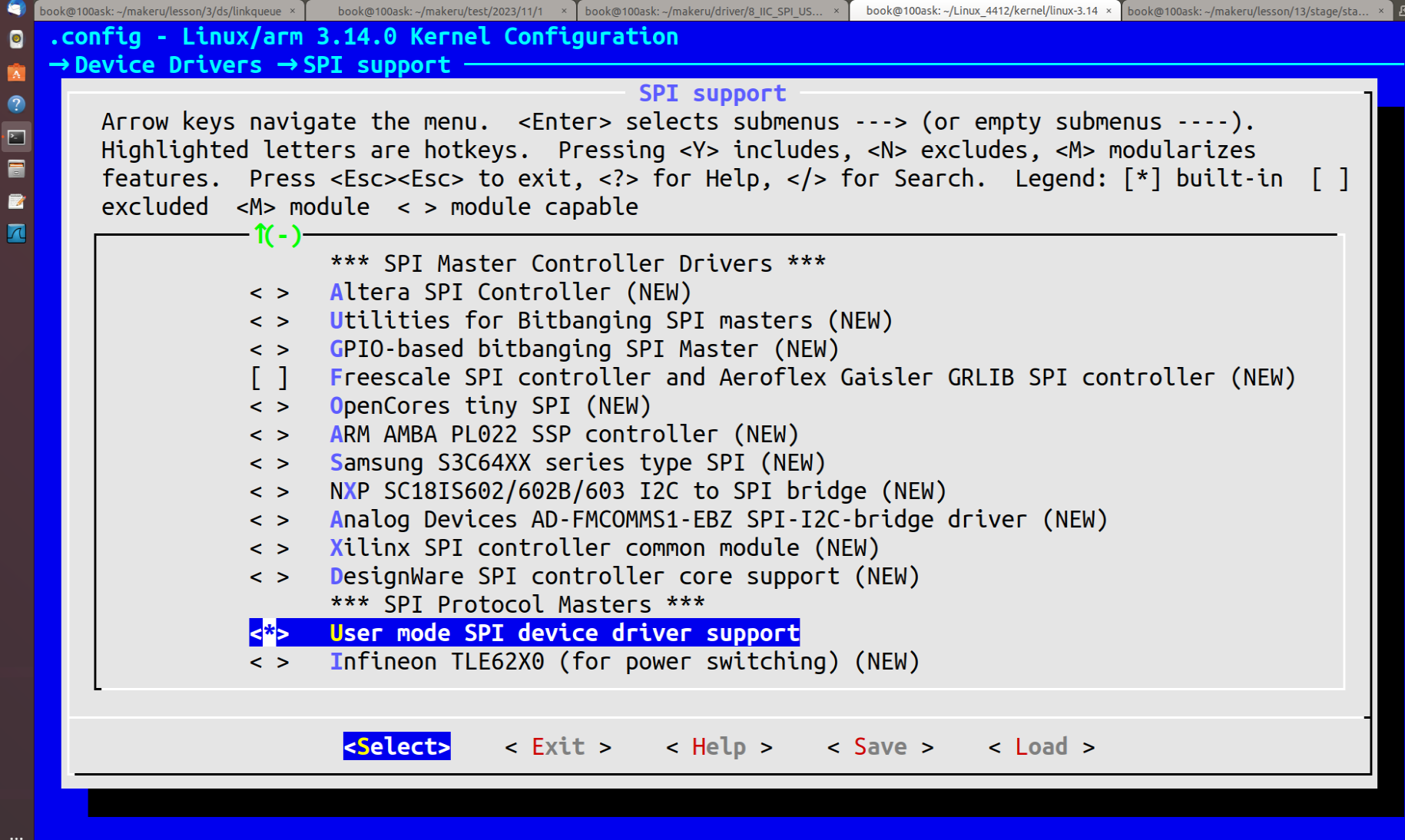
spi_write_then_read: Write n_tx bytes of data in xbuf to the spi device, and then read n_rx bytes of data from the spi device to rxbuf. Return 0 to indicate success, and a negative number to indicate failure. Similar to the I2C driver, a character device can be implemented, and the application program can access the SPI slave device by operating the character device to send and receive data through the SPI host controller. The configuration in the kernel is shown below.
In addition, you also need to add an SPI device node in the device tree to match the spidev driver. The device node contains at least the following content.
SPI application layer driver mainly uses ioctl to operate SPI devices. Commonly used commands are as follows.
SPI_IOC_RD_MODE:Get the mode of the SPI host controller.
SPI_IOC_WR_MODE:Set the mode of the SPI host controller
SPI_IOC_RD_BITS_PER_WORD:Get the SPI word length.
SPI_IOC_WR_BITS_PER_WORD: Set the word length of SPI.
SPI_IOC_RD_MAX_SPEED_HZ: Take the maximum working rate of SPI
SPI_IOC_WR_MAX_SPEED_HZ: Set the maximum working rate of SPI
SPI_IOC_MESSAGE(N): Execute N transmission transactions .
The application layer's data transmission through SPI is also described by messages. The message also contains transmission transactions. The data structure of the application layer's transmission transactions is as follows.
struct spi_ioc_transfer  {
    __u64    tx_buf;
    __u64    rx_buf;

    __u32    len;
    __u32    speed_hz;

    __u16    delay_usecs;
    __u8     bit_per_word;
    __u8     cs_change;
    __u32    pad;

};
tx_buf: Buffer for sending data, it can be NULL if data is not sent
rx_buf: Receive data The buffer that does not receive data can be NULL
len:The number of bytes transmitted.
speed_hz: The operating speed of the host controller when transmitting.
delay_usecs:The delay when the chip select signal is invalid.
bits_per_word:The word length used for transmission.
cs_change:If non-0, it means that the chip select must be invalidated before the next transmission.
pad: is used for structure size control.
The programming steps of the application layer SPI device driver are roughly as follows
(1) Use open to open the /dev /spiB.C device.
(2) Use the ioctl function and the SPI_IOC_WR_MODE, SPI_IOC_WR_BITS_PER_WORD,
SPI_IOC_WR_MA_SPEED_HZ commands to set the working mode, word length and working rate.
(3) Construct the struct spi_ioc_transfer structure object and set the data to be sent and the data length and other information
(4) Use the ioctl function and the SPI_IOC_MESSAGE(N) command to perform the transfer operation. If there is read data, it can be obtained from the receive buffer of the struct spi_ioc_transfer structure object after the SPI_IOC_MESSAGE(N) command is completed. .
(5) When the device is not in use, use close to close the device file
3. SPI device driver example
The code form of the SPI device driver at the application layer is as follows.
....
11 #include <linux/types,h>
12 #include <linux/spi/spidev.h>
13
14 int main(int argc, char **argv)
15 {
16    int fd;
17    unsigned char mode = SPI_MODE_0;
18    struct spi_ioc_transfer xfer[2];
19    unsigned char tx_buf[32];
20    unsigned char rx_buf[32];
21    int status;
22
23    fd = open ("/dev/spidev2.0",O_RDWR);
24    if (fd<0)
25        goto fai1;
26
27    if (ioctl(fd,SPI_IOC_WR_MODE, mode) < 0)
28        goto fail;
29
30    memset(xfer,  0, sizeof(xfer));
31    memset(tx_buf, 0, sizeof(tx_buf));
32    memset(rx_buf, 0, sizeof(rx_buf));
33    tx_buf[0] = 0xAA;
34    xfer[0].tx_buf = (unsigned long)tx_buf;
35    xfer[0].len = 1;
36
37    if(ioctl(fd,SPI_IOC_MESSAGE(1),xfer) < 0)
38        goto fail;
39
40    close(fd);
41
42    return 0;
43
44 fail:
45    perror("spi test");
46    exit(EXIT_FAILURE);
47}
First, the header file linux/spi/spidev.h must be included. Line 23 of the code opens the SPI device file. Line 27 of the code sets the working mode of the SPI host controller to SPI_MODE_0, which depends on the specific SPI device being operated. The relevant content can usually be found in the device's data manual. xfer is a transfer transaction structure object, and one object corresponds to a transfer transaction. Lines 30 to 35 of the code initialize the transmission transaction and initialize the contents of the send buffer. The number of transmission transactions that need to be executed at one time depends on the actual situation. The content of the sending buffer also depends on the actual situation. It is usually some commands to operate the SPI device. Line 37 of the code performs the transfer. Since there is only one transfer transaction, the command is SPI_IOC_MESSAGE(1) and the parameter is xfer, which is the address of the transfer transaction object.
The SPI device driver code form of the kernel layer is as follows.
13 #include <linux/spi/spi.h>
14
15 struct xxx_dev {
16    struct spi_device *spi;
17    atomic_t available;
18    struct cdev cdev;
19 };
20
......

42 static ssize_t xxx_read(struct file *filp, const char __user *buf,  size_t count, loff_t *pos)
43{
44    struct xxx_dev *xxx = filp->private_data;
45    unsigned char rx_buf[256];
46
47    spi_read(xxx->spi, rx_buf, count);
48    copy_to_user(buf, rx_buf, count);
49}
50
5l static ssize_t xxx_write(struct file *filp, const char __user *buf, size_t count, loff_t *pos)
52{
53    struct xxx_dev *xxx = filp->private_data;
54    unsigned char tx_buf[256];
55
56    copy_from_user(tx_buf, buf, count);
57    spi_write(xxx->spi,tx_buf,count);
58}
59
60static long xxx_ioctl(struct file *filp, unsigned int cmd, unsigned long arg)
61{
62    struct xxx_dev *xxx = filp->private_data;
63    unsigned char tx_buf[256];
64    unsigned char rx_buf[256];
65    struct spi_transfer_t = {
66        .tx_buf = tx_buf,
67        .rx_buf = rx_buf,
68        .len = _IOC_SIZE(cmd),
69    };
70    struct spi_message m;
71    int ret;
72
73    switch (cmd) {
74        case XXX_CMD:
75            copy_from_user(tx_buf,(void __user *)arg, __IOC_SIZE(cmd));
76            spi_message_init(&m);
77            spi_message_add_tail(&t,&m);
78            ret = spi_sync(xxx->spi,&m);
79            break;
80        default:
81            return -ENOTTY;
82    }
83
84    return 0;
85}
86
87 static struct file_operations xxx_ops = (
88    .owner = THIS_MODULE,
89    .open = xxx_open,
90    .release = xxx_release,
91    .read = xxx_read.
92    .write = xxx_write,
93    .unlocked_ioctl = xxx_ioctl,
94 };
95
96 static int xxx_probe(struct spi_device *spi)
97{
98     struct xxx_dev *xxx;
99
100    spi->mode = SPI_MODE0;
101    spi->bits_per_word = 8;
102    spi_setup(spi);
103
104
105    xxx = kzalloc(sizeof(struct xxx_dev),GFP_KERNEL);
106    spi_set_drvdata(spi,xxx);
107
108    return 0;
109 }
110
111 static int xxx_remove(struct spi_device *spi)
112{
113    struct xxx_dev *xxx = spi_get_drvdata(spi);
114
115    kfree(xxx);
116    return 0;
117}
118
119 static const struct spi_device_id xxx_id_table[] ={
120    {
121        .name = "xxx",
122    },
123    {}
124};
125 MODULE_DEVICE_TABLE(spi,xxx_id_table);
126
127 static struct spi_driver xxx_driver = {
128    .driver = {
129        .name = “xxx",
130        .owner = THIS_MODULE,
131    },
132    .id_table = xxx_id_tabler
133    .probe = xxx_probe,
134    .remove = xxx_remove,
135 };
136
137 module_spi_driver(xxx_driver);
138
139 MODULE_LICENSE("GPL");
(There is no corresponding sensor on this board, so XXX)
First, you must include the linux/spi/spi.h header file, and include the spi member of type struct spi_device * in the device structure. It is an object pointer pointing to the SPI device. It is passed in in the probe function and saved. It can be used conveniently in the future
Lines 119 to 135 of the code are the device ID table of the SPI driver, the structure definition of the SPI driver, and the registration and unregistration of the driver. This is the same as the previous platform driver and I2C The drivers are very similar.
In the xxx_probe function, the working mode and word length in the SPI device structure object are set, and the SPI host controller is set using spi_setup. The mode and word length need to be determined according to the specific device. Certainly. spi_set_drvdata and spi_get_drvdata in the xxx_remove function are used to set and obtain driver data. There are similar codes in the previous platform driver and I2C driver.
xxx_read function uses spi_read directly to read the SPI device. This is a simplified read operation provided by the kernel. However, how to actually read the SPI data depends on the data manual of the SPI device. Depending on the situation, usually some commands may be sent before the data can be read.
The xxx_write function directly uses the spi_write function to write to the SPI device, but usually, the SPI device will also return some data after receiving the data, such as status information, etc. You can obtain these statuses after writing. , or get the status while writing.
The xxx_ioctl function uses transmission transactions and messages to access SPI devices. This is a more general form. The process is similar to what was mentioned before. First, the transmission transaction is initialized, and then the spi_message_init function is used to initialize the message. Next, spi_message_add_tail is used to add the transmission transaction to the end of the transmission transaction list in the message. Finally, spi_sync is used to synchronously execute the transmission operation and return the data. Can be obtained from the receive buffer of the transmit transaction.
(Since there is no specific use of the corresponding equipment, there will be no actual use. In a few days, when my completed equipment arrives, there will be a physical display and the code and operation corresponding to the actual sensor)