Article directory
1. Introduction
This article introduces an example of implementing a PL-side running water lamp on the ZYNQ 7020 black gold development board. There are a total of 4 LED lights on the PL side of the development board. Find the PL LED in the schematic diagram, as shown in the figure below. By looking at the picture, we can see that the LED The light turns on when the level is set low.

The expected experimental result here is: within 1 second, each of the four LEDs will light up for 0.25 seconds, looking like a running water lamp.
LED: 4, they light up when assigned a value of 0.
Clock: 50MHz.
Reset: active at low level, the key is set to PL KEY1 on the development board.
Count: Add 1 every time the level changes, and reset to 0 after adding to 49999999.
2. Code writing
The creation of the project will not be introduced in detail here, as it has been introduced in previous articles.
The following code is to light up the corresponding LED light when counting to 0, 0.25, 0.5, 0.75 seconds.
`timescale 1ns / 1ps

module led(
    input sys_clk,
    input rst_n,
    output reg[3:0] led
    );

reg[31:0] timer_counter;

always@(posedge sys_clk or negedge rst_n)
begin
    if(!rst_n)
    begin
        led <= 4'b1111;  //置0时灯才亮
        timer_counter <= 32'd0;
    end
    else if(timer_counter == 32'd0)
    begin
        led <= 4'b1110;
        timer_counter <= timer_counter +32'd1;
    end
    else if(timer_counter == 32'd12_500_000)
    begin
        led <= 4'b1101;
        timer_counter <= timer_counter +32'd1;
    end
    else if(timer_counter == 32'd25_000_000)
    begin
        led <= 4'b1011;
        timer_counter <= timer_counter +32'd1;
    end
    else if(timer_counter == 32'd37_500_000)
    begin
        led <= 4'b0111;
        timer_counter <= timer_counter +32'd1;
    end
    else if(timer_counter == 32'd49_999_999)
    begin
        timer_counter <= 32'd0;
    end
    else
    begin
        led <= led;
        timer_counter <= timer_counter +32'd1;
    end
end
endmodule
The functions implemented by the following code are consistent with the above code, and the case statement is introduced.
`timescale 1ns / 1ps

module led(
    input sys_clk,
    input rst_n,
    output reg[3:0] led
    );

reg[31:0] timer_counter;

always@(posedge sys_clk or negedge rst_n)
begin
    if(!rst_n)
    begin
        led <= 4'b1111;
        timer_counter <= 32'd0;
    end
    else if(timer_counter == 32'd49_999_999)
//  else if(timer_counter == 32'd19)  //用于测试
        begin
            timer_counter <= 32'd0;
        end
    else
    begin
        case(timer_counter)
            32'd0          : led <= 4'b1110;
            32'd12_500_000 : led <= 4'b1101;
            32'd25_000_000 : led <= 4'b1011;
            32'd37_500_000 : led <= 4'b0111;
//            32'd0  : led <= 4'b1110;  //用于测试
//            32'd5  : led <= 4'b1101;
//            32'd10 : led <= 4'b1011;
//            32'd15 : led <= 4'b0111;
        endcase
        timer_counter <= timer_counter + 32'd1;
    end
end
endmodule
After the code is written, the system will automatically save it. Pay attention to whether the right sidebar is green or red. If it is green, it means there is no error in the code. Put the mouse on the green box and the following information will be displayed.

If it is red, it means there is an error in the code. There will also be red wavy lines where the code goes wrong, as shown in the figure below.

By the way, the default code font of Vivado is too small. Click Tools->Settings in the menu bar to open the settings window, find Text Editor->Fonts and Colors, and set the font size of the code on the right side.

3. Pin assignment
Click Open Elaborated Design under RTL ANALYSIS on the left to view the schematic diagram, as shown in the figure below.

If there is no I/O Ports at the bottom, you can click the I/O Ports option under Window on the top menu bar to bring it up.

Then refer to the schematic diagram to assign pins to these ports.
Reset is active at low level. Bind it to a button of PL on the development board. As shown in the figure below, select the fourth physical key PL KEY1 on the development board (the first three are reset and two PS respectively. button on the terminal), the corresponding schematic pin is KEY1.

The physical buttons on the PL side on the development board are as shown in the figure below.

The pins corresponding to the four LEDs and the key KEY1 are shown in the figure below.

The clock selected is 50MHz. Find the corresponding name in the schematic diagram, as shown below.

Then find that the pin corresponding to this name is U18, as shown in the figure below.

The VCC3V3 at the top represents 3.3V, so set its VCC to LVCMOS33*, and the allocation is completed as shown in the figure below.

Name and save the file. This file is a constraint file with the suffix xdc. After opening, it is as shown in the figure below.

You can also edit this file later to assign or modify the pins.
Next, run synthesis. After completion, open the Constraint Wizard panel and set the system clock to 50MHz.

At this time, there will be one more line of code in the constraint file, as shown in the figure below.

4. Simulation analysis
Before downloading the bitstream file to the development board, the reason why you simulate it in Vivado software first is because the process of generating the bitstream is too slow. It would be too time-consuming to verify it on the board every time you make a change, so you need to do it in advance. After debugging the code in simulation, you can verify it on the development board when you are confident.
In the code provided above, the code used for testing can reduce the number of counts, so that the simulation time can be shortened during simulation. This has no impact on the overall functional implementation, but remember to change the code when generating the bitstream file. .
The running time of the simulation can be set under Simulation Settings, set here as needed.

Create a new source file for simulation, as shown below.

After completion, write the following simulation test code in the file.
`timescale 1ns / 1ps

module sim_led();
reg sys_clk;
reg rst_n;
wire [3:0] led;

initial
begin
sys_clk = 1;
rst_n = 0 ;
#100;  //延迟100ns
rst_n = 1;
end

//Create clock
always #10 sys_clk = ~ sys_clk; //时钟频率为50MHZ,周期为20ns,因此每延迟10ns,时钟翻转一次

// Instantiate the Unit Under Test (UUT) 例化待测设计
led  uut_led(
	.sys_clk (sys_clk),
	.rst_n (rst_n),
	.led (led)
	);

endmodule
First, use Vivado's own simulation tool to perform a simple behavioral simulation. The results are shown in the figure below. If you are not familiar with the operation of this part of the simulation, you can refer to the article: Use of Simulator simulation software in Vivado .

Through the above simulation, the result is consistent with the preset in the code, then you can verify it on the development board. If the simulation results are inconsistent with your expectations, you need to modify the code and re-simulate until the results are consistent with your expectations, and then verify it on the development board.
5. Add ILA IP
ILA (Integrated Logic Analyzer), that is, integrated logic analyzer, add two probes here, set to 4 bits and 32 bits respectively, corresponding to led and timer_counter in the code. For a detailed introduction to this part, please refer to the article: Using Vivado software for hardware debugging .

After generation, open the ila_0 file and copy the contents of lines 84-90. Pay attention to the digit setting when there are multiple probes. Don’t make mistakes in the code.

Add the following code before endmodule in the led.v file.

The ILA is added.
6. On-board verification
Next, click Generate Bitstream. This will take a long time. After completion, the following dialog box will pop up and select Open Hardware Manager.

Connect the JTAG interface of the development board, power on the development board, and then download the bitstream file to the development board.

After adding ILA, there will also be files here in the Debug probes file.

When the download progress bar is full, it means the download is successful. The demonstration of the PL side water lamp is as shown in the following animation.

Use the integrated logic analyzer to check and set a trigger value of 25000000. You can see that starting from 25000001, the value of the LED changes, as shown in the figure below.
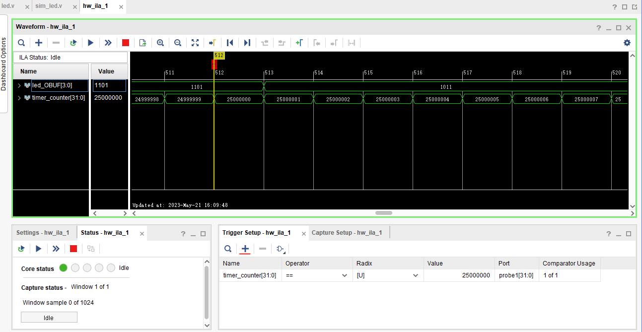
Of course, at 12500000 and 37500000, the LED's value will also change. Through simulation, animation of the LED on the development board, and ILA analysis, the results are output as set in the code.
The above is the entire content of the implementation of ZYNQ-PL side running water lamp!
Reference:
ZYNQ Development Platform FPGA Tutorial AX7020