Table of contents
1. Install Vivado
Official download link:
https://www.xilinx.com/support/download.html
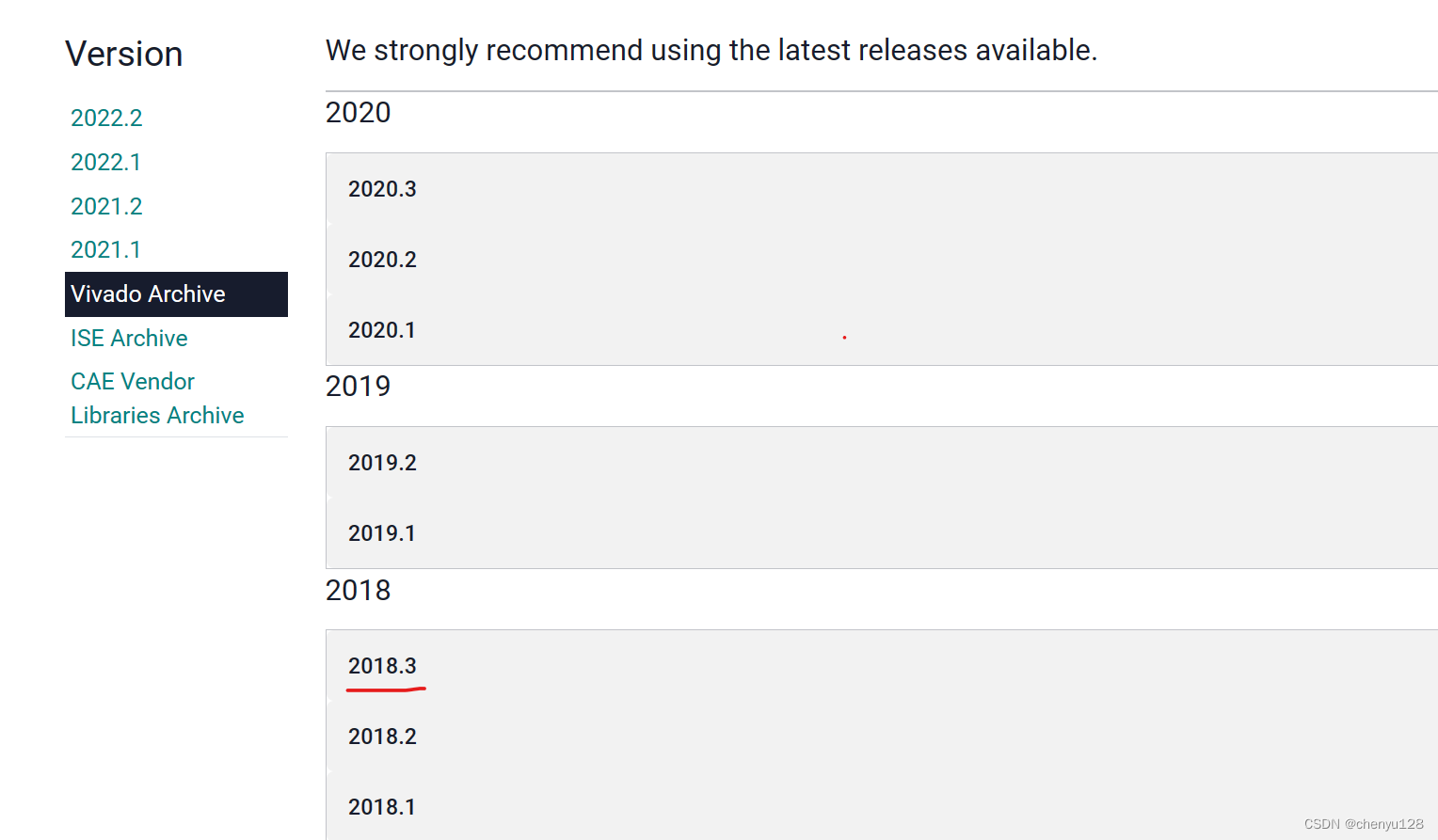
Select the corresponding version to download:
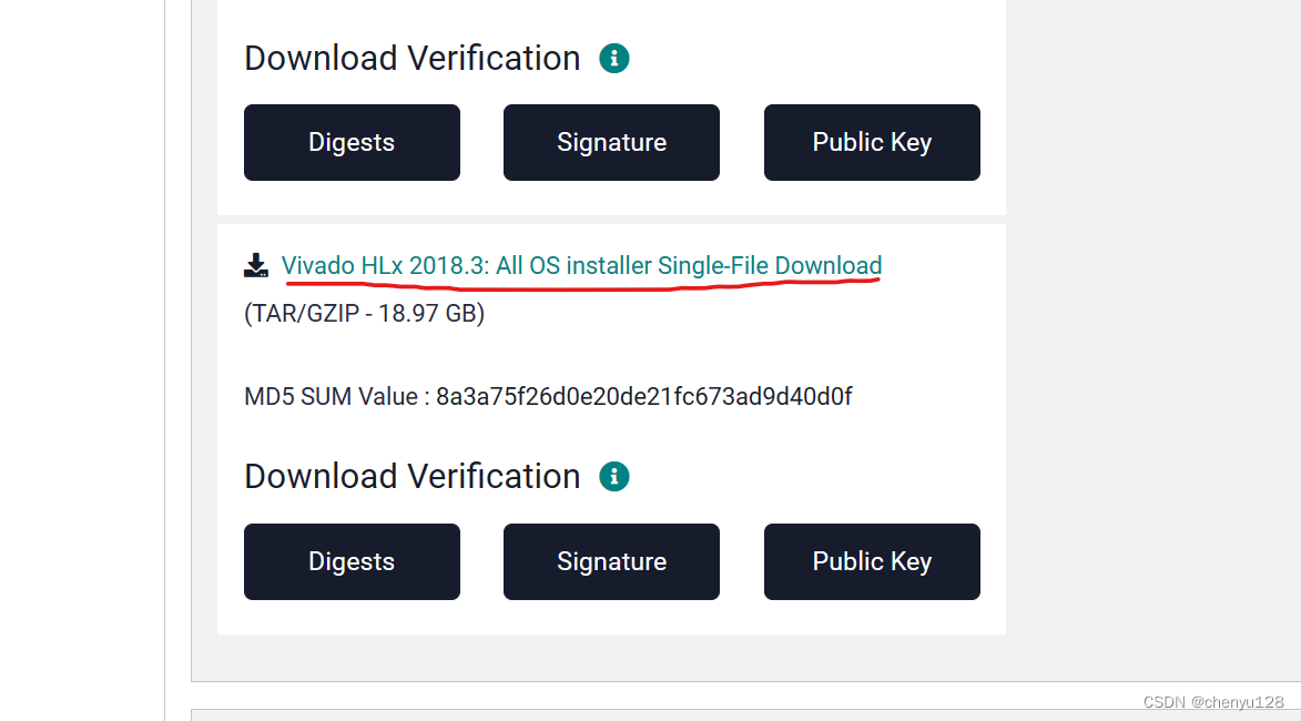
After the download is complete, unzip the folder, double-click xsetup.exe
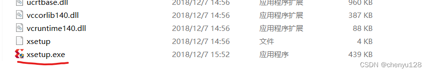
and install it all the way foolishly. Note that the installation path cannot contain Chinese characters and space.
In addition, software license installation is required. The following is the tutorial and documents for installing software license.
https://www.bilibili.com/read/cv15414254/
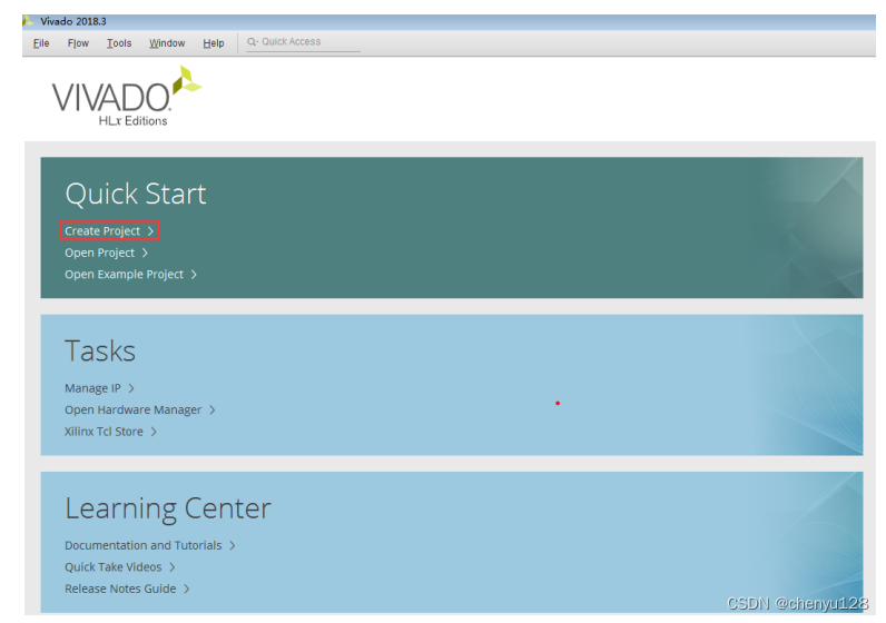
Two, Vivado use process, create a new project
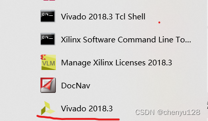
Click Vivado 2018.3,
click Create New Project in the development environment ,
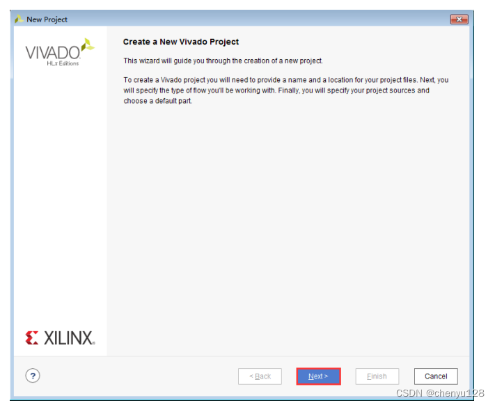
click next
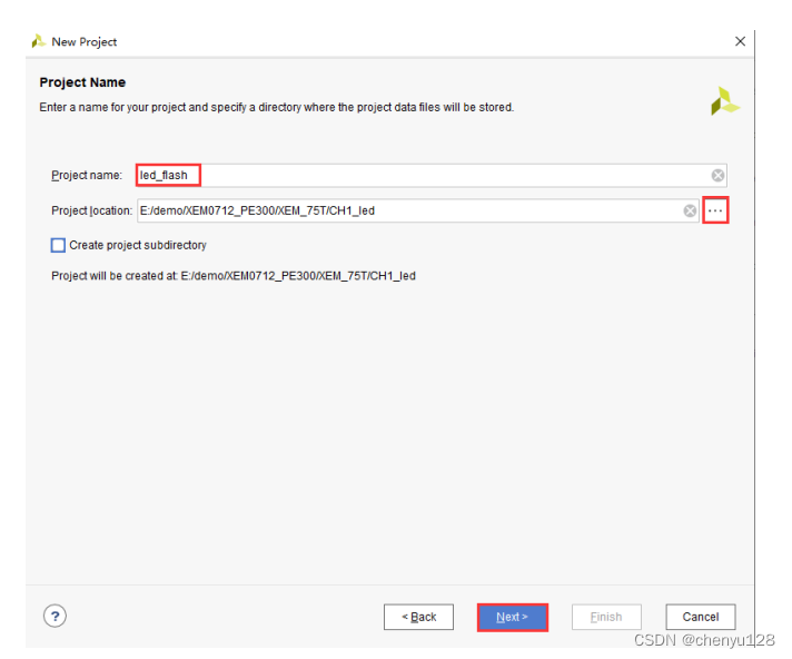
to enter the project name, select the storage path, and then click next
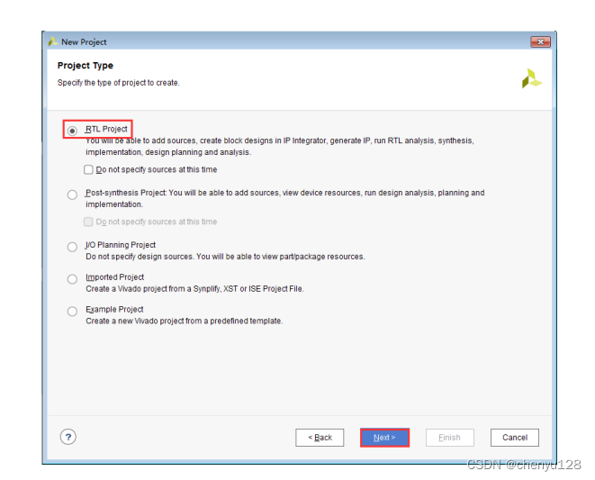
to select the RTL Project, and then click next
. This step is to add the Source file, which will not be added here. Click Next

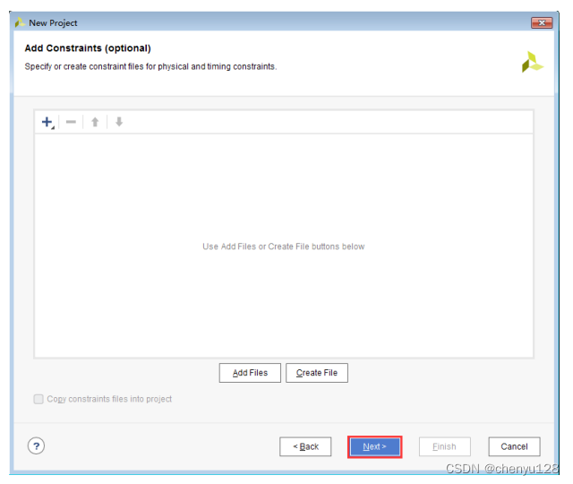
to add the constraint file , also do not add for the time being, click Next
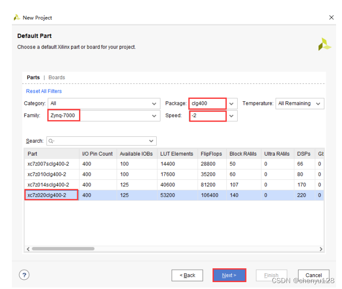
to select the device, you can choose according to the chip model on the development board, because there are many chip models,
you can do some screening.
Z7-Lite7020 users select Zynq-7000 in the Family column, select clg400 in the Package column, and select
the speed grade as 2, and then select the corresponding device in the class table below.
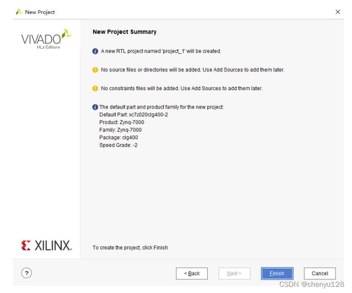
Then click Finish to complete the project creation.
Among
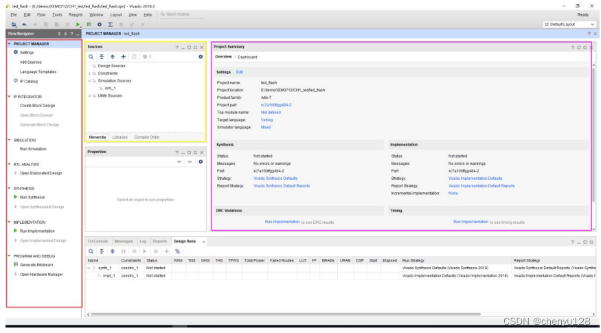
them, the red box is the navigation window of the design process, and each link of FPGA development is from top to bottom. The yellow
frame is the project data file window, where you can view the hierarchical structure of the project and edit the properties of the project file. The purple box
is the main working window, and it has different display contents according to different layouts. The blue frame is the result display window, which displays
the execution results of each link. The black box toggles between different layouts.
3. Programming
1. Create a .V file
Before programming, we need to create a .v program file.
Under the Project Manager on the left sidebar, click the Add Source icon
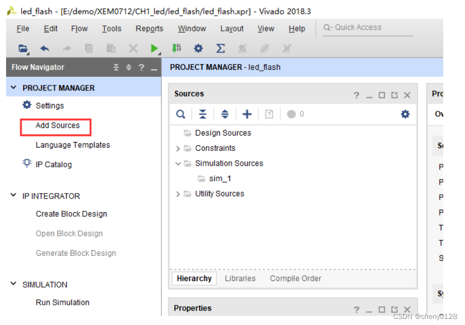
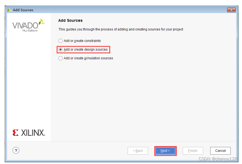
to select Add or Create Design Source, and then click Next.
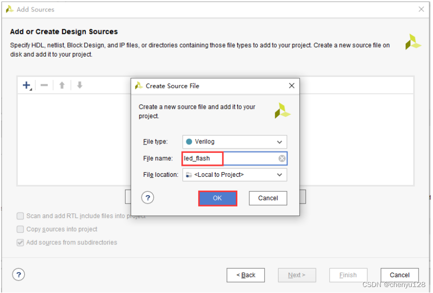
Users can add existing programs. Here we have Program, select Create File

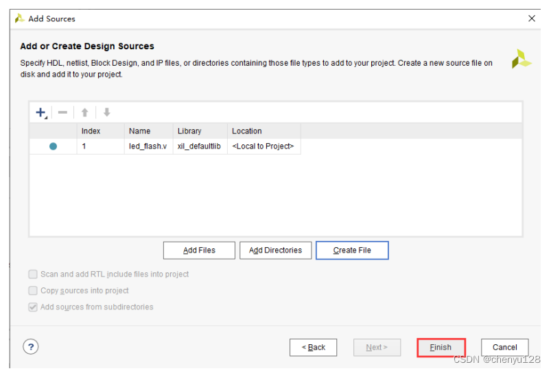
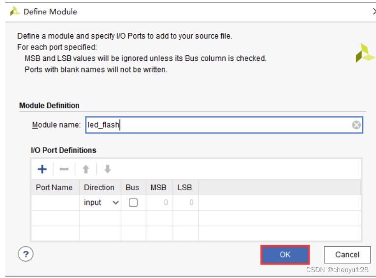
to pop up a dialog box, enter the file name led, click OK
and click Finish to complete
. The wizard will prompt you to define the I/O port, which is not defined here. You can write it in the later program.
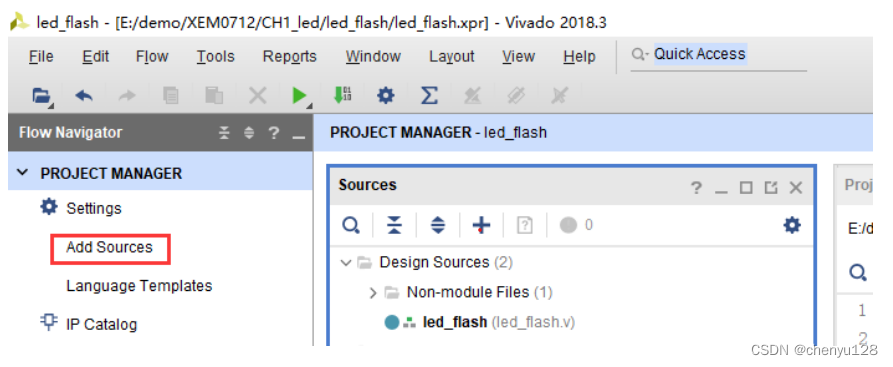
At this time, the Design Source under the Project Manager interface There is a led_flash.v file under it, and
it will automatically become the top module of the project
2. .V file code
The next step is to write the main part of this experiment and complete the part of the running water lamp. code show as below:
`timescale 1ns / 1ps
//
// Company:
// Engineer:
//
// Create Date: 2023/05/14 10:46:26
// Design Name:
// Module Name: led_flash
// Project Name:
// Target Devices:
// Tool Versions:
// Description:
//
// Dependencies:
//
// Revision:
// Revision 0.01 - File Created
// Additional Comments:
//
//


module led_flash(
input       wire      clk,
input       wire      rst_n,
output      reg [1:0] led

    );
reg [27:0]  cnt;
wire        add_cnt;
wire        end_cnt;

always@(posedge clk or negedge rst_n) begin
    if(!rst_n) begin
    cnt<=28'd0;
    end
    else if(add_cnt) begin
    if(end_cnt)
    cnt <= 28'd0;
    else
    cnt <= cnt+1'b1;
    end
end
assign add_cnt = 1;
assign end_cnt = add_cnt && cnt== 10_000_000 - 1;

 //--------------------led--------------------
 always @(posedge clk or negedge rst_n)begin
if(rst_n==1'b0)begin
led <= 2'b10;//reset state
end
else if(end_cnt)begin
led <= {

    led[0], led[1]};
end
else begin
led <= led; //keep the state
end
end
endmodule
Here are some notes on the code: line 12 declares a counter for counting time, and
controls other logic through this counter. Lines 18 to 31 are the implementation code of the counter. The counter remains at 0 at each reset
. After the reset counts, the counter increases by one every clock cycle. When the count reaches the maximum value, the
counter is cleared and restarts counting.
Lines 35 to 45 are the operations to control the flow of LED lights. When reset, the lowest bit of the led is valid. When
the counter counts to the maximum value, the led is shifted. Here, the bit splicing method is used to complete the
shift operation of the led. You can see that the code is very simple.
3. Add discipline constraints
Unlike previous ISE software, the constraint file format used by Vivado is an xdc file. The xdc file
mainly defines pin constraints, clock constraints, and other timing constraints. Here we need to
assign the input and output ports in the led.v program to FPGA pins, which requires adding the .xdc file for pin assignment
to the project
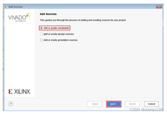
. We need to create a .xdc constraint file first, the left sidebar Under the Project Manager, click
the Add Source icon
to select Add or create constraints, click Next
and click the Create File button, enter the top_pin file name in the file name, click OK and
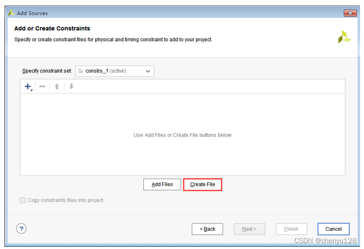
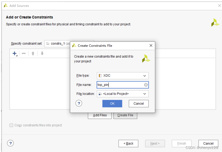
click the Finish button to complete the creation of the constraint file
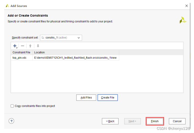
. Open the top_pin.xdc file and add the following constraints, How to write the constraint file, you can refer to
the related documents of xilinx. Let’s introduce the most basic syntax of XDC writing. Ordinary IO ports only need to constrain the pin
number and voltage. The pin constraints are as follows:
set_property PACKAGE_PIN "pin number" [get_ports "port name"]
The constraints for level signals are as follows:
set_property IOSTANDARD "voltage" [get_ports "port name"]
Here you need to pay attention to the capitalization of the text. If the port name is an array, use { } to scrape it up. The port name must be consistent with the name in the source code, and the port name cannot be the same as the keyword. Take the constraint of led[0] as an example:
set_property PACKAGE_PIN G14 [get_ports {led[0]}]
It is to bind the pin of led[0]
set_property IOSTANDARD LVCMOS33 [get_ports {led[0]}]
It is to set the level constraint of led[0].
The constraint files for the Z7-Lite series are as follows:
create_clock -period 20.000 [get_ports clk]
set_property PACKAGE_PIN N18 [get_ports clk]
set_property IOSTANDARD LVCMOS33 [get_ports clk]
############## key define##################
set_property PACKAGE_PIN P16 [get_ports rst_n]
set_property IOSTANDARD LVCMOS33 [get_ports rst_n]
##############LED define##################
set_property PACKAGE_PIN P15 [get_ports {

    led[0]}]
set_property PACKAGE_PIN U12 [get_ports {

    led[1]}]
set_property IOSTANDARD LVCMOS33 [get_ports rst_n]
set_property IOSTANDARD LVCMOS33 [get_ports {

    led[*]}]
set_property IOSTANDARD LVCMOS33 [get_ports clk]
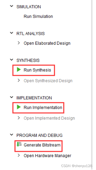
Click 1 to synthesize, 2 to realize, 3 to generate a .bit file, or double-click 3 directly, the effect is the
same
4. Download verification
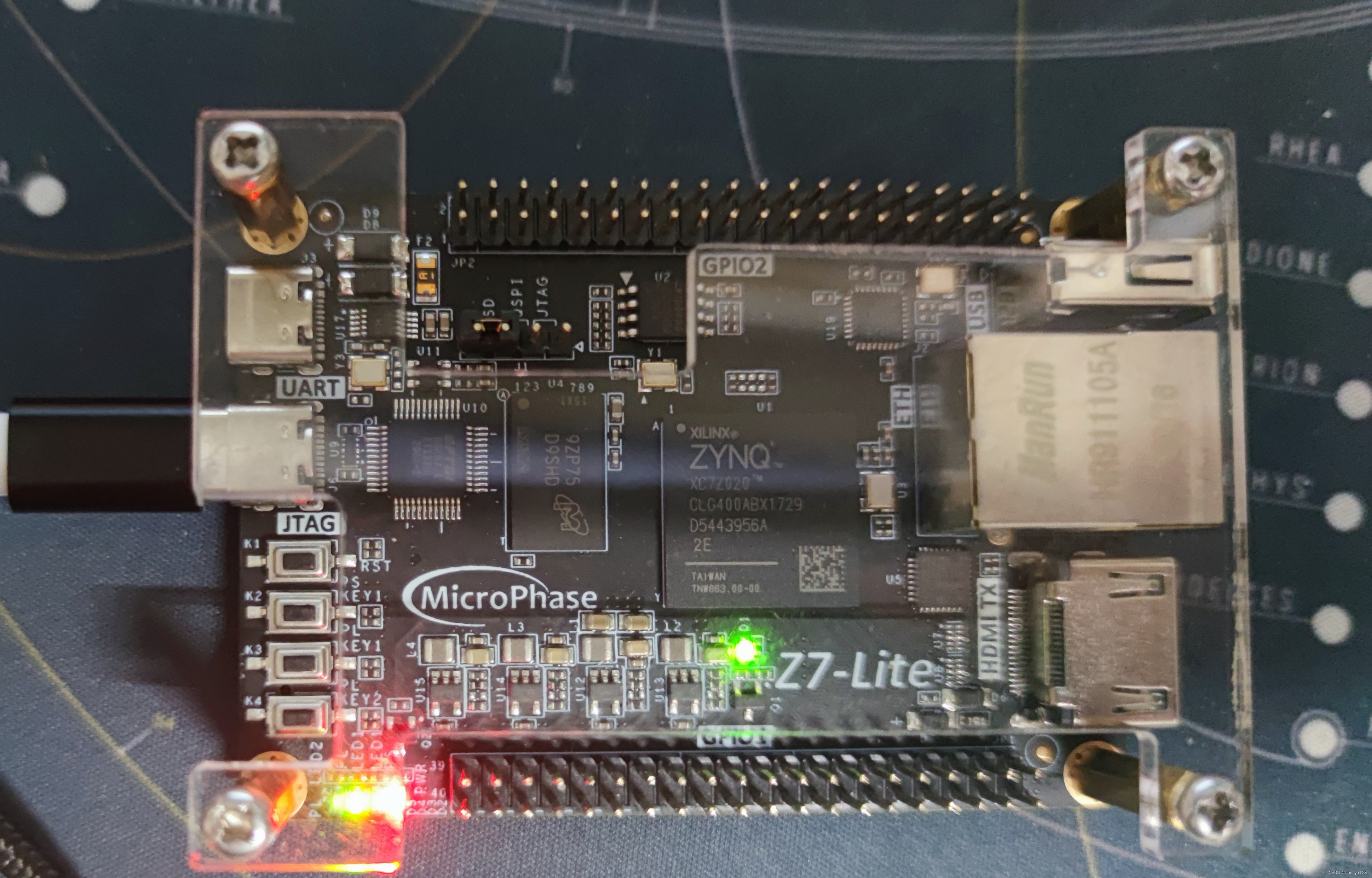
After the .bit file is generated, it can be downloaded to the FPGA chip to see the running results of the LED. Connect
the downloader to the JTAG port and power on the board.
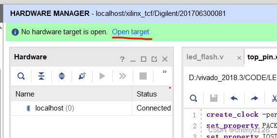
Click Open target
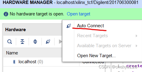
and then click Auto Connect to automatically search for the development board
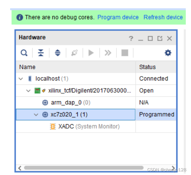
. After the connection is successful, the currently scanned device will be displayed in the Hardware window, as shown in the figure below. The scanned device
is xc7z020, which matches the device model we selected at the beginning.
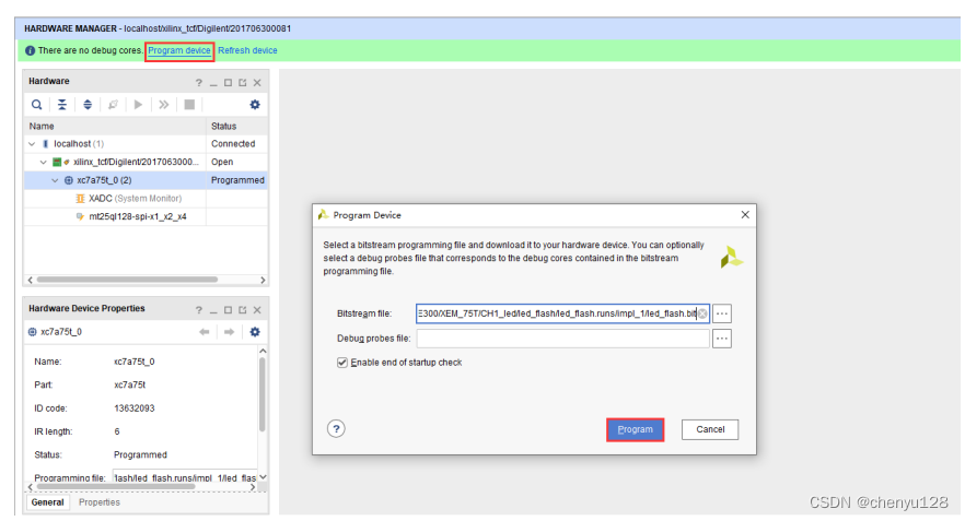
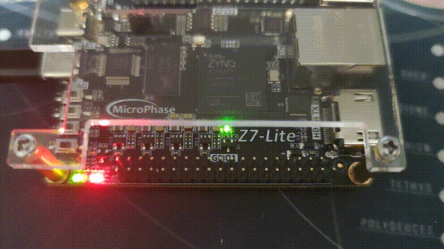
Click Program device, download the program, pop up a dialog box, click the Program button directly.
After the download is complete, you can see 2 led lights start to run the flow operation
4. References
Logic of Part1_Z7_Lite Series Tutorials