Everyone knows that in the chip design industry, projects are a crucial part. From the initial stage of the project to the delivery, what are the engineers in different positions mainly responsible for in each link of the project? How do they cooperate? Let's see what senior engineers say.
For a project, the process from initial stage to delivery is relatively long. We know that at the earliest time, we called it project planning, namely schedule .
This schedule actually talks about what kind of requirements the basic performance of the chip meets, including power consumption, packaging and other related things, which is the project approval, which is the first point. We have said that if your concepts are all wrong, that is, when the project is first defined, for example, if you want to make a high-performance control, your CPU cannot reach such a capability, frankly speaking, your project will not succeed of.
In the second stage, it becomes the detailed design of RTL. This is our requirement for this kind of design engineer . To put it simply, you convert our ideal into a circuit that can be synthesized in the form of HDL, which is our core thing.
Corresponding to the so-called RTL, the functions you compile must ensure at least the correctness of the functions. This part is what we call DFV, or verification engineer . After these parts are settled, the next step is the comprehensive engineer, and the next step is the physical implementation engineer, that is, the back-end design and implementation engineer.
Further down, two engineers will appear. You have to ensure that such a design of yours meets the timing requirements, which is part of it. What is another part we are talking about? It is called PV , that is, physical verification. The accurate progress means that the drawings you design need to meet the design rules defined by the manufacturer. Otherwise, we say that you must not be able to successfully tape out. That is, after you have made such a design, your design cannot be manufactured.
I am basically in such a green area. Although I am a back-end engineer, I deal with RTL engineers every day. We know that as an RTL engineer , you need to accomplish two things. An RTL engineer is not just that you can use and write HDL code, this is not possible. When you make a chip, correct function is your most basic requirement. In addition, you have to meet the performance indicators, as well as the power consumption and area indicators. These points are indispensable.
As far as we are concerned, we think that RTL engineers are actually doing two things. The first thing is to use your own personal skills, such as some kind of HDL. I want to realize such a function, such as a communication chip, a control chip, etc. You have to realize such a basic function.
The second thing is that on the basis of realizing such a function, you need to design the timing. We say that the timing is designed, not the hard work of the back-end engineers. The back-end engineers can only do one thing that is icing on the cake . Sending charcoal in the snow.
We said that back-end engineers can only do this kind of icing on the cake, and cannot reach the level of rebirth, that is, all the roots are in RTL. The last unanimous sentence of everyone is that the root of all problems lies in the design, this is still in brackets, and does not include the errors verified by DFV.
Because we talked about back-end engineers, we actually don't care about functions. There are many people in each circle, and you will know what you are going to do when you get here. There is at least one person in each circle of a project, and it is also a relatively complete process that can guarantee design quality after 20 to 30 years of development.
As we said just now, the root of all problems lies in RTL. For example, after we finish the backend, what should we do if the power consumption exceeds the standard and the area exceeds the standard? In such a case, it must be adjusted through RTL to complete.
The whole team, including front-end and back-end, is still unclear, and they cooperate every day and all the time. This is some of my personal understanding that I want to tell you.
The following is to share with you the project resources in the six major directions
Digital Front End Design
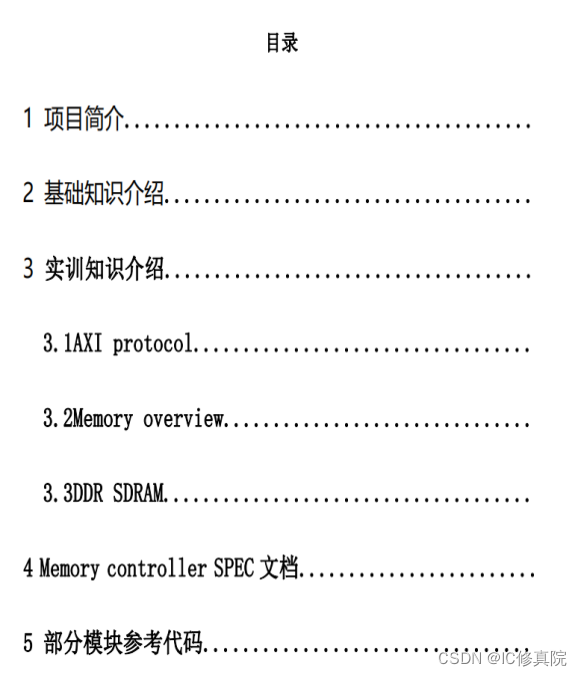
In this project, a memory controller module has been designed to realize the control of array read/write/refresh, and its interface completes the conversion between AXI bus and array interface.
Digital Function Verification
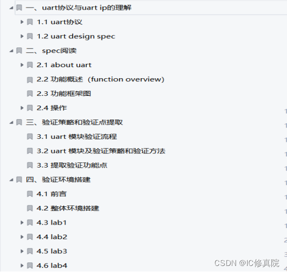
This project is based on the UVM verification platform. As a universal serial data bus, UART is used for asynchronous two-way communication to realize data serial and parallel calls. This UART module supports full-duplex data transmission and reception, data bit 5 8bit, stop bit 1 2bit, parity check, 16 bytes FIFO depth.
Digital DFT Design
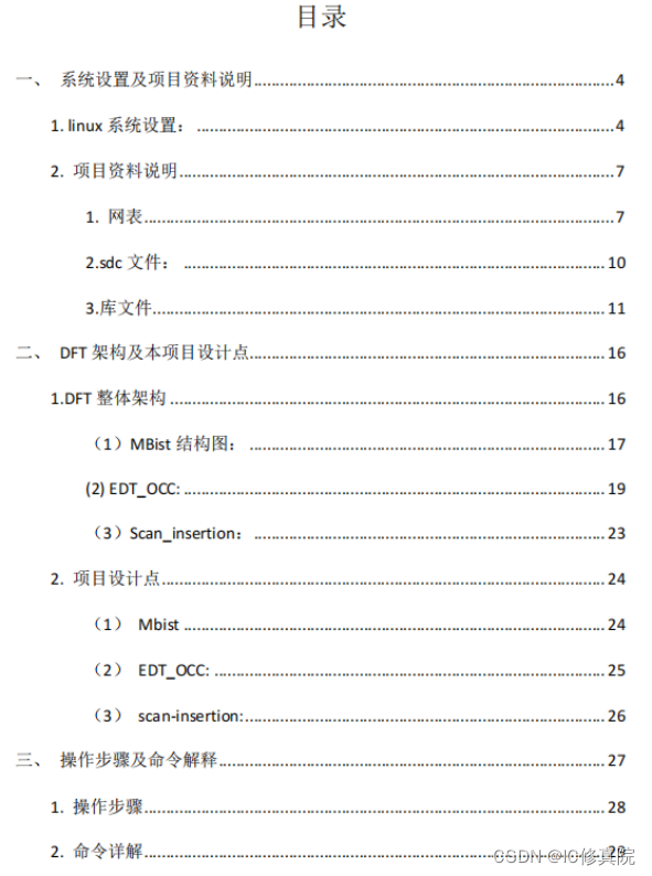
This project is based on tessent, which contains 8W+ registers, and completes the DFT design of the NPU chip that assists the MCU.
Digital Backend Implementation
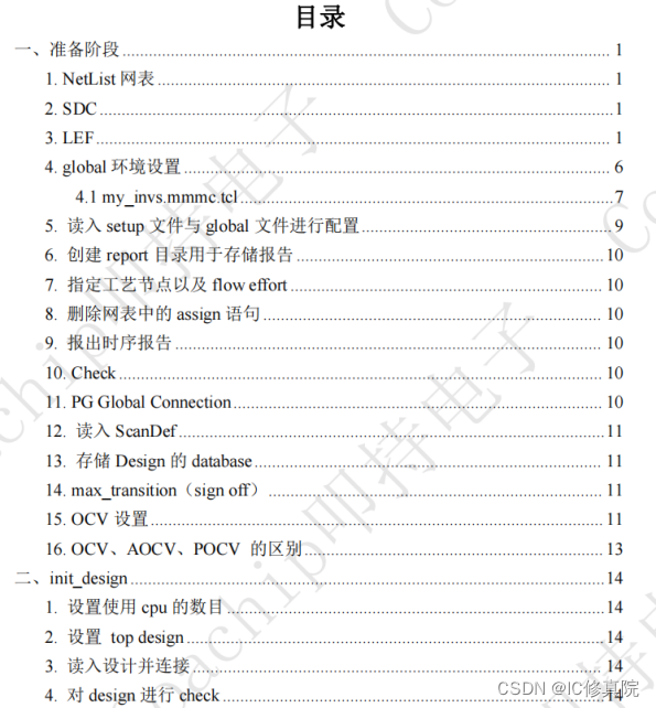
This project is an aes computing module using tsmc28nm technology. The project implementation process covers digital back-end APR, STA, Formal and other processes. The module scale reaches 20W+instance, the working frequency is 500Mhz, and the module size is 1mm*1mm.
Analog IC Design
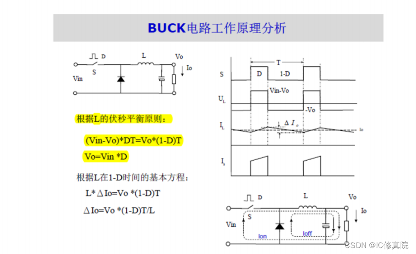
This project designs a switch-type DC voltage converter (Buck), which realizes the step-down conversion of the input DC voltage.
Analog layout
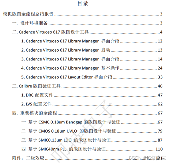
Contains four projects, the design is mainly based on virtuoso 617, completed CSMC 0.18um process Bandgap layout design/CSMC 0.18um process UVLO layout design/SMIC 0.13um process LDO layout design/SMIC 40nm process PLL layout design, and passed layout physical verification , optimize the layout performance according to the device matching rules.
If you have some confusion and intention about entering/changing careers, or want to obtain project resources and study materials for free, the teacher will answer any questions about changing careers for you.
Here is an entry: IC entry guide