Previous episode recap:
[Verilog] Synchronous FIFO principle and verilog implementation
content
1. Scheme design
The asynchronous FIFO uses a completely independent read and write clock, empty is generated by the read clock, and full is generated by the write clock. The relationship between the two is completely asynchronous, so the counter in the synchronous FIFO cannot be used to generate the empty and full signals. In order to solve this problem, a method of converting binary addresses into Gray code addresses is adopted, and then the converted Gray code addresses are used for synchronization across clock domains.
The corresponding circuit diagram is as follows :

The design for judging empty and full is as follows:

2. Verilog code:
module	asyn_fifo#(
	parameter		DATA_WIDTH		=	8,
	parameter		ADDR_WIDTH		=	9
)(
	input							fifo_rst,
	input							rd_clk,
	input							wr_clk,
	input							rd_en,
	input							wr_en,
	input		[DATA_WIDTH-1:0]	wr_data,
	output	reg	[DATA_WIDTH-1:0]	rd_data,
	output	reg						full,
	output	reg						empty
);


reg				[ADDR_WIDTH-1:0]	wr_addr_gray;
reg				[ADDR_WIDTH-1:0]	wr_next_gray;
reg				[ADDR_WIDTH-1:0]	rd_addr_gray;
reg				[ADDR_WIDTH-1:0]	rd_next_gray;
reg				[ADDR_WIDTH-1:0]	rd_last_gray;
reg				[ADDR_WIDTH-1:0]	rd_addr;
reg				[ADDR_WIDTH-1:0]	wr_addr;
reg		[DATA_WIDTH-1:0]	ram		[ADDR_WIDTH-1:0];
wire			rd_allow		;
wire			wr_allow        ;
wire			emptyg		    ;
wire			almost_empty    ;
wire			fullg		    ;
wire			almost_full	    ;

assign			rd_allow	=	(rd_en  && !empty);
assign			wr_allow	=	(wr_en  && !full );
assign			emptyg		=	(wr_addr_gray  ==  rd_addr_gray);
assign			almost_empty=	(wr_addr_gray  ==  rd_next_gray);
assign			fullg		=	(wr_addr_gray  ==  rd_last_gray);
assign 			almost_full	=	(wr_next_gray  ==  rd_last_gray);

always @ (posedge rd_clk or posedge fifo_rst)begin
	if(fifo_rst)
		empty	<=	1'b1;
	else
		empty	<=	(emptyg || (almost_empty && rd_en && !empty));
end
always @ (posedge rd_clk or posedge fifo_rst)begin
	if(fifo_rst)
		full	<=	1'b1;
	else
		full	<=	(fullg || (almost_full && wr_en && !full));
end
//read
always @ (posedge rd_clk or posedge fifo_rst)begin
	if(fifo_rst)begin
		rd_addr	<=	'b0;
		rd_data	<=	'b0;
		end
	else if(rd_allow)begin
		rd_addr <= 	rd_addr + 1'b1;
		rd_data	<=	ram[rd_addr];
		end
end
always @ (posedge rd_clk or posedge fifo_rst)begin
	if(fifo_rst)
		rd_next_gray	<=	9'b100_000_000;
	else if(rd_allow)
		rd_next_gray 	<=	 {rd_addr[8],(rd_addr[8]^rd_addr[7]),(rd_addr[7]^rd_addr[6]),
							(rd_addr[6]^rd_addr[5]),(rd_addr[5]^rd_addr[4]),(rd_addr[4]^rd_addr[3]),
							(rd_addr[3]^rd_addr[2]),(rd_addr[2]^rd_addr[1]),(rd_addr[1]^rd_addr[0])};
end
always @ (posedge rd_clk or posedge fifo_rst)begin
	if(fifo_rst)
		rd_addr_gray	<=	9'b100_000_001;
	else if(rd_allow)
		rd_addr_gray 	<=	rd_next_gray;
end
always @ (posedge rd_clk or posedge fifo_rst)begin
	if(fifo_rst)
		rd_last_gray	<=	9'b100_000_011;
	else if(rd_allow)
		rd_last_gray 	<=	rd_addr_gray;
end
//write
always @ (posedge wr_clk or posedge fifo_rst)begin
	if(fifo_rst)begin
		wr_addr	<=	'b0;
		//ram[wr_addr]	<=	'b0;
		end
	else if(wr_allow)begin
		wr_addr <= wr_addr + 1'b1;
		ram[wr_addr]	<=	wr_data;
		end
end
always @ (posedge wr_clk or posedge fifo_rst)begin
	if(fifo_rst)
		wr_next_gray	<=	9'b100_000_000;
	else if(wr_allow)
		wr_next_gray	<=	 {wr_addr[8],(wr_addr[8]^wr_addr[7]),(wr_addr[7]^wr_addr[6]),
							(wr_addr[6]^wr_addr[5]),(wr_addr[5]^wr_addr[4]),(wr_addr[4]^wr_addr[3]),
							(wr_addr[3]^wr_addr[2]),(wr_addr[2]^wr_addr[1]),(wr_addr[1]^wr_addr[0])};
end
always @ (posedge wr_clk or posedge fifo_rst)begin
	if(fifo_rst)
		wr_addr_gray	<=	9'b100_000_001;
	else
		wr_addr_gray	<=	wr_next_gray;
end

endmodule
3. Simulation
write:
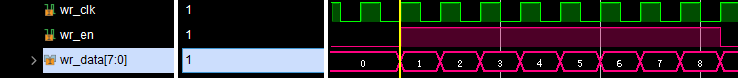
Write 1-8, read 1-8
read out:

PS: I have been busy recently, and the quality of the blog has declined, sorry.
This is a Huawei design I saw before. I came to a set of notes. The code seems to have bugs. I have time to study it on the weekend.