Memory-mapped I/O
In our first lab, we will add hardware (IP Cores) to the PL to extend the functionality of the PS. This lab guides you through the process of extending the processing system by adding two GPIO (General Purpose Input/Output) IPs. GPIO provides a general purpose input/output interface to any external peripheral that you want to include in your design. In this lab, GPIOs will be connected to the push buttons and LEDs available on the ZedBoard.The General Purpose Master Interface (M_AXI_GP0) of the PS will be enabled, GPIO peripherals will be added to the PL side and connected to the processing system through the AXI Interconnect block. The peripherals will be configured and external connections to the outside world will be established. The following figuress (Click on the figures to enlarge) illustrate that:

Lab1 Design Flow

Lab1 Block Diagram

Lab1 Board Interface
A software application “lab1.c” will be running on one of the ARM processor in the PS. The application is responsible for initializing and configuring the GPIOs to display a binary count on the LEDs. It will continuously read the push buttons status and control the direction and speed of the LED’s blinking according to the button being pressed.
Objectives of this lab
1.Setting up Vivado to target the Zynq SoC Family and more specifically the Zedboard, which we will be using as a development and testing board.
2.Creating an embedded processor project using the IP Integrator. IP stands for (Intellectual Property ). IP Integrator is a graphical tool within Vivado that provides an easy,yet intelligent way to add hardware components(which is commonly referred as IP).
3.Configuring the ZYNQ7 Processing System using the Re-customizing window, this includes deciding the clock frequencies for different components in the processing system, interrupt, reset settings, how many processors needed, what are the peripherals to include, whether programmable logic is needed or not , and if needed what kind of interface is required.
4.Adding soft IPs in the PL, the AXI GPIO will be added. It provides a general purpose input/output interface, the AXI GPIO can be configured as either a single or a dual-channel device, and the width of each channel is independently configurable. In addition to the GPIO, the AXI Interconnect will be added as well, which is responsible for connecting the ARM processor in the PS to the AXI GPIO. AXI is the protocol of communication between the ARM processor and the different peripherals.
5.Supporting the master AXI interface on the PS side to communicate with AXI Interconnect on the PL side.
6.Configuring the reset and clock signals used by different IPs.
7.Configuring the width and direction of the AXI GPIO IPs.
8.Learning how to make connections (for data and control) between the different IPs and the PS.
9.Learning Designer Assistance features to automate connections between IPs.
10.Learning how to make external connections to allow the Zynq chip to connect to the outside world.
11.Assigning identifiers (addresses) for the different IPs to be able to uniquely identify and utilize them in software.
12.Creating constraints, mainly to specify which components on the board to be associated with the external connections we defined in the block diagram.
13.Using Block Automation features of Vivado to generate device and board aware physical constraints.
14.Performing system validation, by which we can catch some common design errors.
15.Generating Bitstream file to program the PL side of the chip.
16.Understanding how Vivado tools summarize the hardware configuration process in several few files : ps7_init.c, ps7_init.h, ps7_init.tcl, and ps7_init.html, having an insight of what is being saved in each one of these files.
17.Introducing Xilinx SDK (Software Development Kit ) to provide a neat and scalable approach for developing software applications targeting the Zynq SoC Family.
18.Developing a basic standalone application “lab1.c”,standalone applications do not utilize an Operating System (OS). They are sometimes also referred to as bare-metal applications. Standalone applications have access to basic processor features such as caches, interrupts, exceptions as well as other simple features specific to the processor. These basic features include standard input/output, profiling, abort, and exit. It is a single threaded environment.
Procedures
A-Create a project in Vivado to target the Zedboard
1.Launch Vivado Design Suite.
2.Click on File-> New Project,to open New Project Wizard then click Next.

New Project Wizard
3.In the next window enter “lab1” as the Project Name, specify the directory in which to store the project files ”c:/embeddedcentric/”- create the folder “embeddedcentric” in your C: drive, which will contain all lab’s files, leave the Create Project Subdirectory option checked.

Project Name and Location
4.Next, specify the project type, Use the default selection RTL Project and check Do not specify sources at this time. RTL stands for Register Transfer Language, by choosing this option we will have the flexibility to add/modify source files later on as needed.

Project Type
5.Next, specify the board that you want to test your project on, for all the labs on Zynq Soc Training we will use the Zedboard Zynq Evaluation and Development Kit version D. Click Next,then click Finish.

Default Part
The New Project wizard closes and the project you just created opens in Vivado. The board you choose in the wizard has a direct impact on how IP Integrator functions. IP Integrator is board aware and will automatically assign dedicated PS ports to physical pin locations mapped to that specific board. It also applies the correct I/O standard, saving the designer’s time.

Vivado Interface
B- Create an embedded processor project using the IP Integrator
1.Click on the Create Block Design in the Project Manager available on the left top side of Vivado.
2.Type a name for the module and click OK. Use the name: “system”.

Create Block Design
3.After clicking OK you will be presented a blank block diagram view in the Vivado graphical user interface. In the blank diagram you can add and connect the hardware blocks that you need in your design.
4.Now, we will add ZYNQ7 Processing System block. By adding this block, you can configure one of the ARM Cortex-A9 processor cores for your application. This is done by launching the Add IP wizard![]() . The IP catalog window will appear showing you all IPs that can be added in this design
. The IP catalog window will appear showing you all IPs that can be added in this design

IP Catalog
Either scroll down to the very bottom or search using the keyword “zynq”, double click on ZYNQ7 Processing System. The ZYNQ7 Processing System block has been placed in the block diagram view. The ports shown on the block diagram are defined by the default settings for this block as specified by target development board.

Default Ports
C- Configure the ZYNQ7 Processing System
The ZYNQ7 Processing System block allows you to edit any property of the Zynq PS, this includes clock frequency settings, reset polarities, interrupts, memory interfaces, I/O peripherals and more. For this lab, we will do some basic configuration to include only the necessary hardware needed to run the application “lab1“ which controllers two GPIOs.
1.Double click on the ZYNQ7 Processing System block to edit the settings (Recustomize the IP). The Re-customize window of the ZYNQ7 Processing System (5.5) will show up. The Page navigation contains the following pages:
PS-PL Configuration: Configuring processing system –programmable logic Interface (if any), we have four possible methods for interfacing the PS-PL, which one to select is actually a decision made with regards to the bandwidth and the size of the data to be exchanged between the two.
Peripheral I/O Pins and MIO configuration: The Zynq-7000 PS has over 20 hard peripherals controllers available. You can route these peripherals directly to the dedicated Multiplexed I/Os (MIO) on the device, or through the Extended Multiplexed I/Os (EMIOs) routing to the fabric(PL). These interfaces also lets you select I/O standards and slew settings for the I/O. The I/O peripheral block appears with a checkmark when you enable a peripheral. The block design depicts the status of enabled and disabled peripherals.
Clock Configuration: Different peripheral could run on different clocks, the Clock Configuration tab configure different clock domains in the Zynq-7000 device.
DDR Configuration: Configure all aspects related to the DDR, which is the main memory of the board.
SMC timing calculation: Static Memory Controller information that can be used as primary boot device.
Interrupts: Configure both PL->PS and PS -> PL interrupts.
Note : The Page Navigator pages on the left hand side provides the PS properties that can be edited, you can always reset these setting back to the default values by clicking on Presets button in the top bar then select the ZedBoard Development Board Template
2.Click on the MIO Configuration page under the Page Navigator. Expand I/O Peripherals and select UART1( We will use the UART as a serial terminal for the ARM processor).

Enabling UART1
3.Click on the Clock Configuration page, expand PL Fabric Clocks, and make sure FCLK_CLK0 is selected.Enter 100 in the Requested Frequency(Mhz) field. We will be using the PL fabric in this lab, and hence we need to feed it a clock signal.

Enabling PL Fabric Clock
4.Click on the PS-PL Configuration page, expand AXI Non Secure Enablement, expand GP Master AXI Interface. make sure M AXI GP0 interface is selected. We will be using the PL in this lab so it would be necessary to provide a channel to communicate with it, hence it makes sense to enable the interface logic.

Enabling GP Master AXI Interface
5.Also within the PS-PL Configuration page, expand General > Enable Clock Resets, make sure FCLK_RESET0_N is selected. This will be the reset for the logic within the PL. Click OK to exit the Re-Customize IP window.

Enabling Clock Reset
Click Run Block Automation in the green information bar. The Run Block Automationcan assist you in generating external connections for the peripherals included in the design. Make sure to deselect the option Apply Board Preset otherwise all the customization we just did will be overwritten. Click OK.

Generating External Connections for the UART
Notice that FIXED_IO and DDR are now connected to output ports. Vivado made external connections for the FIXED_IO which in our case contains the connections of the USB-UART chip available on the board (RX and TX pins). Also, it made connections to the DDR memory address bus, data bus and control signals. The DDRmemory is needed to store “lab1.c” and its software package.

PS connected to DDR memory and USB-UART chip available on board
D- Adding IPs in the PL-side
1.Click on the Add IP button. From the IP catalog, double-click AXI GPIO to add it.You can type the name ” gpio” in the search field. Notice the block has been automatically added to the block diagram.

Adding GPIO
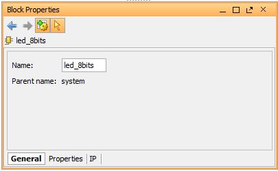
2.Click on the AXI GPIO block to select it, and in the properties tab change the name to led_8bits.
Changing the GPIO name to led_8bits
3.Double click on the AXI GPIO block to open the customization window, and under Board, for GPIO, click on Custom to view the dropdown menu options, and select leds_8bits. Click OK to save and close the customization window. As the Zedboard was selected during the project creation wizard( Step A-5), and a board support package is available for the Zedboard, Vivado has knowledge of available resources on the board. By choosing this option the wizard will automatically set the width and direction of the IP to 8 bits width output.

Customizing GPIO led_8bits
4.Notice that Designer Assistance is available in the upper left side of the diagram viewer, Click on Run Connection Automation, and select GPIO and S_AXI. Click OKwhen prompted to automatically connect the slave interfaces of the GPIO to the master interface of the PS through the AXI Interconnect block ( which will be added by Vivado automatically). The Designer Assistance feature allows you to automatically connect port(s) of an IP to suitable port(s) of another IP available in the design efficiently.

Run Connection Automation
Notice two additional blocks, Processor System Reset, and AXI Interconnect have automatically been added to the design.

System after adding the first GPIO IP
You can always click the Regenerate Layout ![]() available in diagram viewer toolkit to get a neat view of the blocks and connections.
available in diagram viewer toolkit to get a neat view of the blocks and connections.
The Designer Assistance has automatically added the necessary hardware and wiring needed to connect a GPIO in the PL-side to the PS saving us a lot of time(as we will see later when we do this process manually!). The AXI Interconnect is a central unit in this design as it connects a single master device (The ARM processor) to two memory-mapped slave peripherals (GPIO) , while Processor System Reset provides a mechanism to handle multiple reset conditions in the system.
5.Click on the Add IP button again, to add another AXI GPIO to the system.
6. Click on the IP, and in the block properties menu that will be activated , rename the block to “btns_5bits”.

Changing the GPIO name btns_5bits
At this point, Designer Assistance could be run to connect the newly added IP to the system like we did before with the LEDs, but instead we will do that manually for reasons discussed in later paragraphs .
E-Connecting the bnts_5bits GPIO to the system manually( Without using Designer Assistance)
I-External Connection
1.Double click on the btns_5bits AXI IP to open its customization window. In the IP configuration window, set the GPIO width to 5( As we want to connect it to five push buttons available in the bottom right corner of Zedboard) .Check All Input ( buttons are input devices). A GPIO could also be configured to have two channels, however, we will be using only one for this lab with no interrupt support . Click OK.

Manually customizing GPIO btns_5bits
2.Right Click on the GPIO port of btns_5bits instance and select Make External to create an external port. This will create the external port named GPIO and connect it to the peripheral.

Manually making an external connection
3.Select the GPIO port and change its name to btns_5bits in its properties tab.

Naming the btns_5bits external port
II-Internal Connection
1.Double click on the AXI Interconnect. Change the Number of Master Interfaces to 2 and click OK.

Changing the Number of Master Interfaces of AXI Interconnect to 2
2.Click on the S_AXI port of btns_5bits block, and drag the pointer. Message Found 1interface should appear, and a green tick should appear beside the M01_AXI port on the AXI Interconnect indicating this is a valid port to connect to. Drag the pointer to this port and release the mouse button to make the connection.

Connecting btns_5bits internally
3.In a similar way, connect the following signals:
Component Signal Component Signal
btns_5bits s_axi_aclk -> Zynq7 Processing System FCLK_CLK0
btns_5bits s_axi_aresetn -> Processor System Reset peripheral_aresetn
AXI Interconnect M01_ACLK -> Zynq7 Processing System FCLK_CLK0
AXI Interconnect M01_ARESETN -> Processor System Reset peripheral_aresetn
The block diagram should look something similar to this:

System after connecting GPIO btns_5bits
You can always click the Regenerate Layout ![]() available in diagram viewer toolkit to get a neat view of the blocks and connections.
available in diagram viewer toolkit to get a neat view of the blocks and connections.
F-Assigning addresses to memory-mapped devices
Inside IPs (among other hardware components) are data and control registers, which a processor can read/write from/to, therefore, for a an ARM-based system, IPs should be memory-mapped in order for a processor to access their registers. Each memory-mapped device (IP) should have a unique identifier. This unique identifier is known as the base address or Offset Address of the device, which represents the mapping of its registers in address space. To assign an Offset Address to the IPs used in this design, Click on the Address Editor tab, then click on the Auto Assign Address button.

Address Editor
Note: Because we had used the Designer Assistance on led_8bits it was already assigned an Offset Address.
A message will be prompted saying all IPs have been assigned addresses . Click OK. The Address Editor should now look like this:

Address Editor after Auto Assign Address
G-Validating the design
Since we are using the PL side of the Zynq chip in this lab, we need to generate a Bitstream file to configure the PL. An important step to be performed prior to Bitstream generation is the Validation, by which we can catch some design errors, For example, the frequency on a clock pin may be set incorrectly. The tool can catch these types of errors by running design validation. Validating the design runs design rule checks on the block design and reports warnings and/or
errors that are applicable to the design. You can then cross-probe the warnings and/or errors from the messages view into the block diagram. Xilinx recommends validating a board design to catch design errors that would otherwise be unnoticed until later in the design flow.
To validate the design (Tools -> Validate Design) and verify there are no errors or warnings .

Validate Design
Click the Save button to save the current block diagram, after doing that, move to the Sources pane, Right click on system.bd and select Create HDL Wrapper to create the top level Verilog file from the block diagram. Select Let Vivado manage wrapper and auto-update when prompted with the next message. Notice that system_wrapper.v got created and placed at the top of the design sources hierarchy.

Create HDL Wrapper
H-Assigning physical constraints
The external port we have defined in part ‘E-I-2’ is called unconstrained connections,this is because the btns_5bits GPIO is connected from one side while the other side is loss “connected to nothing “ i.e unconstrained . To make the other side connected to something we need to use physical constraints, which make these ports connected to actual pinss of the Zynq chip.
1.In the Flow Navigator, click Run Synthesis![]() (This will take some time) and when synthesis completes, select Open Synthesized Design and click OK.
(This will take some time) and when synthesis completes, select Open Synthesized Design and click OK.
2.In the toolbar at the top, select I/O Planning from the Layout dropdown menu, this will open up the Package view of the chip ( the bottom side of the chip).

I/O Planning
Bottomside of a chip
Now we need to find out which pins on the chip are connected to the push buttons, to find such information we need to look it up in the Zedboard manual, google “ZedBoard user manual”

Finding ZedBoard User Manual
Open the pdf file, and search for “User I/O”. You will find the following information:

Zedboard UserIO Connections
The Signal name represents the component’s name as printed on the Zedboard, while the Zynq EPP* pin represents the pin name of the Zynq chip this component is connected to. In the I/O Ports, make the adjustment to the SITE and I/O std as specified below:

Physical constraints for the Zedboard push buttons
*EPP stands for Extensible Processing Platform, which was the initial name of what is known now as All programmable System on Chip- SoC .
Note : Steps (E)Connecting the bnts_5bits GPIO to the system manually( Without using Designer Assistance), (F)Assigning addresses to memory-mapped devices and (H)Assigning physical constraints are the result of not using the Designer Assistance in connecting bnts_5bits GPIO to the system. Two reasons why I took the long way and didn’t use the Designer Assistance. First :This is the standard approach to connect customized IP cores ( IP cores that you design or get from a 3rd party). Designer Assistance is limited when dealing with IP cores that you design or get from a 3rd party. The second reason is to appreciate what the Designer Assistance is doing and to understand what is happening behind the scenes.
I-Generating Bitstream
Since we are using the PL side of the Zynq chip in this lab, we need to generate a Bitstream file to configure the PL. In the Program and Debug list in the Flow Navigatorpane, click Generate Bitstream.

Generating Bitstream
A dialog box will appear to ask you to save the modification you made , click Save, also you might get a dialog that says synthesis is not run on the updated files, click OK. a save Constrains window might appear choose Create New file and give it the name “system” and click OK.

Saving Constraints
Another message that says synthesis is not run on the updated files might pop up. Click Yes to rerun synthesis. Generating the Bitstream may invoke the entire implementation process after synthesis, click Yes to run implementation when prompted. .You may get dialogue boxes notifying you of critical warnings during implementation, click OK to ignore them. Do not stop the runs. After the Bitstream generation completes, select Open Implemented Design in the dialog box and click OK. This allows you to get a graphical overview of the PL resource usage and routing.
J-Exporting hardware design to SDK
Software applications development for the Zynq platform is done separately in a dedicated toolkit called SDK (Software Development Kit), after defining the hardware system needed for your project you can export that design to SDK so you can develop applications dedicated for that specific architecture, this can be done by following these steps:
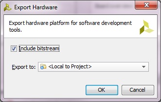
1.Click File > Export > Export Hardware.
2.The Export Hardware dialog box opens. Make sure to check Include Bitstream, Click OK to continue.
Export Hardware to SDK
3.Go back to the File menu and select Launch SDK. The Launch SDK dialog box will pop up, leave the default settings and click OK.
By now, we are done with the hardware side. Let’s move to the software side. You may close Vivado.
K-Working with SDK
Now, you can start developing software for your project using SDK. Vivado has exported the Hardware Platform Specification for your design (system.xml in this example) to SDK. In addition to system.xml, there are four more files relevant to SDK that got created and exported. They are ps7_init.c, ps7_init.h, ps7_init.tcl, and ps7_init.html.
The system.xml file opens by default when SDK is launched. The address map of your system is shown by default in the SDK window, as well as any IP blocks present in the system. The ps7_init.c and ps7_init.h files contain the initialization code for the Zynq Processing System and any initialization settings for DDR, clocks, plls, and MIOs. SDK uses these settings when
initializing the processing system so that applications can be run on top of the processing system.

SDK Interface
Now let’s start creating an application for our design :
1.In SDK, select File > New > Application Project.
2.In the next window that shows enter “lab1” as the name of the project , Check the Use default location to save the application file in the same directory as your SDK project, for the Hardware Platform select system_wrapper_hw_platform_0 which represents the hardware specification we previously defined in Vivado, select ps7_cortexa9_0 ( remember we have two processors in the Zynq ). As for the OS platform, we will use the basic standalone since no advance Operating System features are required. We will be writing our applications using C. Create a new board support package and name it “lab1_bsp” in case you want to use it in another project. Click Next, the next window will show you a fully-functioning available templates of C codes that we can used for testing purposes, choose Empty Application from the Available Templates then Click Finish. By doing so, lab1 application project and lab1_bsp BSP project get created under the project explorer.

Creating a Standalone C Application Project
3.Expand lab1 directory , right click on the src directory , New->Source File

New C Source File
4.In the next window that shows up type “lab1.c” in the source file and click Finish. This will create an empty C file in the src directory.

Create an Empty C Source File lab1.c
5.Paste the content of lab1.c ( Available on my Github page) in in the editor view of lab1.c of SDK , and click on Save ![]() or hit (Ctrl+S) , by doing so both the lab1 application, and its BSP are compiled automatically and the executable .elf file is generated( the default settings of SDK triggers compilation with save). This is the executable file that the ARM processor on the PS side of the Zynq chip will execute. lab1.c tasks can be summarized with the following :
or hit (Ctrl+S) , by doing so both the lab1 application, and its BSP are compiled automatically and the executable .elf file is generated( the default settings of SDK triggers compilation with save). This is the executable file that the ARM processor on the PS side of the Zynq chip will execute. lab1.c tasks can be summarized with the following :
a.Initialize the GPIOs for both the push buttons and the LEDs.
b.Set the direction of the push buttons GPIO to all inputs.
c.Set the direction of the LEDs GPIO to all output.
d.Execute an infinite loop for reading the push buttons status to select between different setting of speed and direction for the LEDs blinking.
e. Write to the LEDs.
f.Create a software delay ( To make the blinking visible to the human eye)
For information on the GPIO driver APIs you can refer to to gpiops.h available in the include directory of lab1_bsp .

Compile the Application and its BSP
6.We will be using a serial communication terminal between the Zedboard and the host computer, to configure this terminal we will use a program called Putty . After installing it. Open Putty, select the connection type to be Serial, for the Serial linecheck the port associated to the USB-UART in the Device Manager ( it may vary from one machine to another ) , speed : 115200 and click Open.

Serial line on my machine ( USB-UART port)

Putty Settings
A black window will open up, which represents the standard output of the ARM processor on the Zedboard, we will use this terminal as a way to see what is going on( This was possible by using print statements in the C application – check lines 46,91,94,95 of the C source code) at the Zedboard side, we might also use it for debugging in future labs.
7.Now we are ready to configure the PL-side of the chip with the Bitstream and run application lab1 on the ARM processor. The configuration of the PS-side is done using the ps7_init.tcl file that was generated when you imported your design into SDK; it contains the initialization information for the processing system. When using JTAG, this configuration file will be executed once you download the application.
L-Downloading the Bitstream & Launching the Application
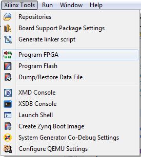
1.Select Xilinx Tools-> Program FPGA to download the Bitstream, leave the default options as is, and click Program ( this will take few seconds ).
Downloading Bitstream to the PL
2.Select lab1 project directory-> Run As-> Launch on Hardware (GDB) to run the lab1 application on the ARM processor.

Launch Application
You should see a similar output on Putty, the LEDs on the board should be blinking to represent a binary count:

Putty Output
The 8 LEDs on the Zedboard are now emitting the variable “out” value in binary. For example, when “out” is equal to 26. which in binary (00011010). The LEDs will emit the following pattern :

LEDs Output
The value of “out” is bounded to the range (0-255) , which in 8-bits binary (00000000-11111111). You can control whether “out” is increasing or decreasing using the up and down push buttons respectively. The speed of the blinking can be also controlled using the ( left , middle , right ) push buttons, left is the slowest speed, while right is the fastest leaving middle in the middle. See the demo Video.
By this you have completed Lab1-Memory-mapped I/O. You can find the complete solution of this lab in here.