Open-Drain、Push-Pull、floating input
在配置GPIO(General Purpose Input Output)管脚的时候,常会见到两种模式:开漏(open-drain,漏极开路)和推挽(push-pull)。对此两种模式,有何区别和联系,下面整理了一些资料,来详细解释一下:
一、Push-Pull推挽输出
1、原理
输出的器件是指输出脚内部集成有一对互补的MOSFET,当Q1导通、Q2截止时输出高电平;而当Q1截止导通、Q2导通时输出低电平。Push-Pull输出,实际上内部是用了两个晶体管(transistor),此处分别称为Top-Transistor和Bottom-Transistor。通过开关对应的晶体管,输出对应的电平。Top-Transistor打开,Bottom-Transistor关闭,输出为高电平;Bottom-Transistor打开,Top-Transistor关闭,输出低电平。Push-pull即能够漏电流(sink current),又可以集电流(source current)。其也许有,也许没有另外一个状态:高阻抗(high impedance)状态。除非Push-pull需要支持额外的高阻抗状态,否则不需要额外的上拉电阻。
2、特点
在CMOS电路里面应该叫CMOS输出更合适,因为在CMOS里面的push-pull输出能力不可能做得双极那么大。输出能力看IC内部输出极N管、P管的面积。push-pull是现在CMOS电路里面用得最多的输出级设计方式。
3、优点
(1)可以吸电流,也可以贯电流;
(2)push-pull输出的优势是速度快,因为线路是以两种方式驱动的
(3)和开漏输出相比,push-pull的高低电平由IC的电源决定,不能简单的做逻辑操作等。
4、缺点
(1)一条总线上只能有一个push-pull输出的器件;
(2)push-pull往往需要消耗更多的电流,即功耗相对大。
二、Open-Drain开漏输出
1、原理
开漏电路是指以MOSFET的漏极为输出的电路,在内部输出和地之间有个N沟道的MOSFET(Q1),这些器件可以用于电平转换的应用。输出电压由Vcc决定。Vcc可以大于输入高电平电压VCC (call UP-Translate),也可以低于输入高电平电压VCC(call Down-Translate),Open-Drain比push-pull少了个top transistor,只有bottom transistor。就像push-pull中那样,当bottom transistor关闭,则输出为高电平。此处没法输出高电平,想要输出高电平,必须外部再接一个上拉电阻(pull-up resistor)。Open-drain只能够漏电流(sink current),如果想要集电流(source current),则需要加一个上拉电阻。
2、优点
(1)对于各种电压节点间的电平转换非常有用,可以用于各种电压节点的Up-translate和Down-translate转换
(2)可以将多个开漏输出的Pin脚,连接到一条线上,形成“与逻辑”关系,即“线与”功能,任意一个变低后,开漏线上的逻辑就为0了。这也是I2C,SMBus等总线判断总线占用状态的原理。
(3)利用外部电路的驱动能力,减少IC内部的驱动。当IC内部MOSFET导通时,驱动电流是从外部的VCC流经pull-up resistor,MOSFET到GND。IC内部仅需很小的栅极驱动电流。
(4)可以改变上拉电源的电压,改变传输电平,如图所示,IC的逻辑电平由电源Vcc1决定,而输出高电平则由Vcc2决定。这样我们就可以用低电平逻辑控制输出高电平逻辑了。
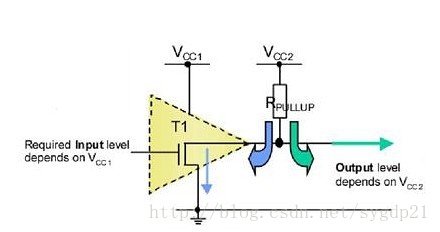
OD输出电平的原理
3、缺点
(1)开漏Pin不连接外部的上拉电阻,则只能输出低电平,如果要输出高电平,必需加上拉电阻。
(2)带了上拉电阻的线路,即使以最快的速度去提升电压,最快也要一个常量的R×C的时间。其中R是电阻,C是寄生电容(parasitic capacitance),包括了pin脚的电容和板子的电容。
(3)当输出电平为低时,N沟道三极管是导通的,这样在Vcc和GND之间有一个持续的电流流过上拉电阻R和三极管Q1,这会影响整个系统的功耗。采用较大值的上拉电阻可以减小电流。但是大的阻值会使输出信号的上升时间变慢,即上拉电阻的阻值决定了逻辑电平转换的沿的速度。阻值越大,速度越低功耗越小,反之亦然。但上拉电阻不能太小,因为当输出为低电平的时候,需要sink更低的transistor,这意味着更高的功耗。
三、open-drain和push-pull的总结
对于GPIO的模式的设置,在不考虑是否需要额外的上拉电阻的情况下,是设置为open-drain还是push-pull,说到底,还是个权衡的问题:
如果你想要电平转换速度快的话,那么就选push-pull,但是缺点是功耗相对会大些。
如果你想要功耗低,且同时具有“线与”的功能,那么就用open-drain的模式。(同时注意GPIO硬件模块内部是否有上拉电阻,如果没有,需要硬件电路上添加额外的上拉电阻)
正所谓,转换速度与功耗,是鱼与熊掌,二则不可兼得焉。
四、open drain and push-pull
The push-pull output actually uses two transistors. Each will be on to drive the output to the appropriate level: the top transistor will be on when the output has to be driven high and the bottom transistor will turn on when the output has to go low.
The open-drain output lacks the top transistor. When the output has to go high you simply turn off the bottom transistor, but the line is now pulled high only by the pullup resistor.
Your micro allows you to select between the two types, which means that by setting some bits in some register you actually enable/ disable the top transistor and enable/disable the pullup (if internal, otherwise you just disable the top transistor and have to use an external pullup).
The advantage of the push-pull output is the higher speed, because the line is driven both ways. With the pullup the line can only rise as fast as the RC time constant allows. The R is the pullup, the C is the parasitic capacitance, including the pin capacitance and the board capacitance.
The push-pull can typically source more current. With the open-drain the current is limited by the R and R cannot be made very small, because the lower transistor has to sink that current when the output is low; that means higher power consumption.
However, the open-drain allows you to cshort several outputs together, with a common pullup. This is called an wired-OR connection. Now you can drive the output low with any of the IO pins. To drive it high all ouputs have to be high. This is advantageous in some situations, because it eliminates the external gates that would otherwise be required.
五、floating input
A "floating" input is one that is not "tied" to anything: hence "floating".
The usual "tie-ing" is either a pull-up resistor to the power rail or a pull-down resistor to 0 volts / gnd. Either of these connections establishes a known potential at the input. Without either, the input potential is indeterminable - so it is "floating." In terms of electronic engineering and almost without exception, floating inputs are recognised as bad practice.
